VisionCB-x2L-STD Datasheet and Pinout: Difference between revisions
From SomLabs Wiki
| (28 intermediate revisions by the same user not shown) | |||
| Line 288: | Line 288: | ||
{| class="wikitable" | {| class="wikitable" | ||
! style="text-align: center; font-weight: bold;" | Console line | ! style="text-align: center; font-weight: bold;" | Console line | ||
! style="text-align: center; font-weight: bold;" | | ! style="text-align: center; font-weight: bold;" | MPU signal | ||
! style="text-align: center; font-weight: bold;" | GPIO | ! style="text-align: center; font-weight: bold;" | GPIO | ||
! style="text-align: center; font-weight: bold;" | Description | ! style="text-align: center; font-weight: bold;" | Description | ||
|- | |- | ||
| CONSOLE-TXD || UART0- | | CONSOLE-TXD || UART0-RXD || P38-1 || GPIO 3.3V voltage levels | ||
|- | |- | ||
| CONSOLE-RXD || UART0- | | CONSOLE-RXD || UART0-TXD || P38-0 || GPIO 3.3V voltage levels | ||
|} | |} | ||
</center> | </center> | ||
| Line 361: | Line 361: | ||
| P12-0 | | P12-0 | ||
| P12-0 | | P12-0 | ||
| GPIO 3. | | GPIO 3.3V voltage levels | ||
|- | |- | ||
| 12 | | 12 | ||
| P13-1 | | P13-1 | ||
| P13-1 | | P13-1 | ||
| GPIO 3. | | GPIO 3.3V voltage levels | ||
|- | |- | ||
| 13 | | 13 | ||
| P7-2 | | P7-2 | ||
| P7-2 | | P7-2 | ||
| GPIO 3. | | GPIO 3.3V voltage levels | ||
|- | |- | ||
| 14 | | 14 | ||
| P11-0 | | P11-0 | ||
| P11-0 | | P11-0 | ||
| GPIO 3. | | GPIO 3.3V voltage levels | ||
|- | |- | ||
| 15 | | 15 | ||
| P48-2 | | P48-2 | ||
| P48-2 | | P48-2 | ||
| GPIO 3. | | GPIO 3.3V voltage levels | ||
|- | |- | ||
| 16 | | 16 | ||
| P4-1 | | P4-1 | ||
| P4-1 | | P4-1 | ||
| GPIO 3. | | GPIO 3.3V voltage levels | ||
|- | |- | ||
| 17 | | 17 | ||
| CAN1-RX | | CAN1-RX | ||
| P13-0 | | P13-0 | ||
| GPIO 3. | | GPIO 3.3V voltage levels | ||
|- | |- | ||
| 18 | | 18 | ||
| CAN1-TX | | CAN1-TX | ||
| P12-1 | | P12-1 | ||
| GPIO 3. | | GPIO 3.3V voltage levels | ||
|} | |} | ||
| Line 442: | Line 442: | ||
| P45-0 | | P45-0 | ||
| P45-0 | | P45-0 | ||
| GPIO 3. | | GPIO 3.3V voltage levels | ||
|- | |- | ||
| style="vertical-align:bottom;" | 8 | | style="vertical-align:bottom;" | 8 | ||
| style="vertical-align:bottom;" | UART4-TXD | | style="vertical-align:bottom;" | UART4-TXD | ||
| P2-0 | | P2-0 | ||
| style="vertical-align:bottom;" | GPIO 3. | | style="vertical-align:bottom;" | GPIO 3.3V voltage levels | ||
|- style="vertical-align:bottom;" | |- style="vertical-align:bottom;" | ||
| 9 | | 9 | ||
| Line 457: | Line 457: | ||
| style="vertical-align:bottom;" | UART4-RXD | | style="vertical-align:bottom;" | UART4-RXD | ||
| P2-1 | | P2-1 | ||
| style="vertical-align:bottom;" | GPIO 3. | | style="vertical-align:bottom;" | GPIO 3.3V voltage levels | ||
|- style="vertical-align:bottom;" | |- style="vertical-align:bottom;" | ||
| 11 | | 11 | ||
| P8-2 | | P8-2 | ||
| P8-2 | | P8-2 | ||
| GPIO 3. | | GPIO 3.3V voltage levels | ||
|- style="vertical-align:bottom;" | |- style="vertical-align:bottom;" | ||
| 12 | | 12 | ||
| P15-0 | | P15-0 | ||
| P15-0 | | P15-0 | ||
| GPIO 3. | | GPIO 3.3V voltage levels | ||
|- style="vertical-align:bottom;" | |- style="vertical-align:bottom;" | ||
| 13 | | 13 | ||
| P14-1 | | P14-1 | ||
| P14-1 | | P14-1 | ||
| GPIO 3. | | GPIO 3.3V voltage levels | ||
|- style="vertical-align:bottom;" | |- style="vertical-align:bottom;" | ||
| 14 | | 14 | ||
| Line 482: | Line 482: | ||
| P14-0 | | P14-0 | ||
| P14-0 | | P14-0 | ||
| GPIO 3. | | GPIO 3.3V voltage levels | ||
|- style="vertical-align:bottom;" | |- style="vertical-align:bottom;" | ||
| 16 | | 16 | ||
| UART1-RXD | | UART1-RXD | ||
| P40-0 | | P40-0 | ||
| GPIO 3. | | GPIO 3.3V voltage levels | ||
|- style="vertical-align:bottom;" | |- style="vertical-align:bottom;" | ||
| 17 | | 17 | ||
| P11-1 | | P11-1 | ||
| P11-1 | | P11-1 | ||
| GPIO 3. | | GPIO 3.3V voltage levels | ||
|- style="vertical-align:bottom;" | |- style="vertical-align:bottom;" | ||
| 18 | | 18 | ||
| UART1-TXD | | UART1-TXD | ||
| P40-1 | | P40-1 | ||
| GPIO 3. | | GPIO 3.3V voltage levels | ||
|- style="vertical-align:bottom;" | |- style="vertical-align:bottom;" | ||
| 19 | | 19 | ||
| SPI0-MOSI | | SPI0-MOSI | ||
| P43-1 | | P43-1 | ||
| GPIO 3. | | GPIO 3.3V voltage levels | ||
|- style="vertical-align:bottom;" | |- style="vertical-align:bottom;" | ||
| 20 | | 20 | ||
| Line 512: | Line 512: | ||
| SPI0-MISO | | SPI0-MISO | ||
| P43-2 | | P43-2 | ||
| GPIO 3. | | GPIO 3.3V voltage levels | ||
|- style="vertical-align:bottom;" | |- style="vertical-align:bottom;" | ||
| 22 | | 22 | ||
| P9-1 | | P9-1 | ||
| P9-1 | | P9-1 | ||
| GPIO 3. | | GPIO 3.3V voltage levels | ||
|- style="vertical-align:bottom;" | |- style="vertical-align:bottom;" | ||
| 23 | | 23 | ||
| SPI0-CLK | | SPI0-CLK | ||
| P43-0 | | P43-0 | ||
| GPIO 3. | | GPIO 3.3V voltage levels | ||
|- style="vertical-align:bottom;" | |- style="vertical-align:bottom;" | ||
| 24 | | 24 | ||
| SPI0-SSL | | SPI0-SSL | ||
| P43-3 | | P43-3 | ||
| GPIO 3. | | GPIO 3.3V voltage levels | ||
|- style="vertical-align:bottom;" | |- style="vertical-align:bottom;" | ||
| 25 | | 25 | ||
| Line 537: | Line 537: | ||
| P9-0 | | P9-0 | ||
| P9-0 | | P9-0 | ||
| GPIO 3. | | GPIO 3.3V voltage levels | ||
|- | |- | ||
| 27 | |||
| I2C3-SDA | |||
| P46-2 | |||
| I2C | | I2C interface used by MPU for SOM PMIC configuration | ||
|- | |- | ||
| 28 | |||
| I2C3-SCL | |||
| P46-3 | |||
| I2C | | I2C interface used by MPU for SOM PMIC configuration | ||
|- | |- | ||
| 29 | | 29 | ||
| UART1-CTS | | UART1-CTS | ||
| P41-0 | | P41-0 | ||
| GPIO 3. | | GPIO 3.3V voltage levels | ||
|- style="vertical-align:bottom;" | |- style="vertical-align:bottom;" | ||
| 30 | | 30 | ||
| Line 562: | Line 562: | ||
| UART1-RTS | | UART1-RTS | ||
| P41-1 | | P41-1 | ||
| GPIO 3. | | GPIO 3.3V voltage levels | ||
|- style="vertical-align:bottom;" | |- style="vertical-align:bottom;" | ||
| 32 | | 32 | ||
| P1-1 | | P1-1 | ||
| P1-1 | | P1-1 | ||
| GPIO 3. | | GPIO 3.3V voltage levels | ||
|- style="vertical-align:bottom;" | |- style="vertical-align:bottom;" | ||
| 33 | | 33 | ||
| P10-1 | | P10-1 | ||
| P10-1 | | P10-1 | ||
| GPIO 3. | | GPIO 3.3V voltage levels | ||
|- style="vertical-align:bottom;" | |- style="vertical-align:bottom;" | ||
| 34 | | 34 | ||
| Line 582: | Line 582: | ||
| SPI1-MISO | | SPI1-MISO | ||
| P44-2 | | P44-2 | ||
| GPIO 3. | | GPIO 3.3V voltage levels | ||
|- style="vertical-align:bottom;" | |- style="vertical-align:bottom;" | ||
| 36 | | 36 | ||
| SPI1-SSL | | SPI1-SSL | ||
| P44-3 | | P44-3 | ||
| GPIO 3. | | GPIO 3.3V voltage levels | ||
|- style="vertical-align:bottom;" | |- style="vertical-align:bottom;" | ||
| 37 | | 37 | ||
| P10-0 | | P10-0 | ||
| P10-0 | | P10-0 | ||
| GPIO 3. | | GPIO 3.3V voltage levels | ||
|- style="vertical-align:bottom;" | |- style="vertical-align:bottom;" | ||
| 38 | | 38 | ||
| SPI1-MOSI | | SPI1-MOSI | ||
| P44-1 | | P44-1 | ||
| GPIO 3. | | GPIO 3.3V voltage levels | ||
|- style="vertical-align:bottom;" | |- style="vertical-align:bottom;" | ||
| 39 | | 39 | ||
| Line 607: | Line 607: | ||
| SPI1-CLK | | SPI1-CLK | ||
| P44-0 | | P44-0 | ||
| GPIO 3.3 voltage levels | | GPIO 3.3V voltage levels | ||
|} | |||
== GMII of ETH0 connection == | |||
[[File:VisionCB-x2L-STD-GMII-ETH0.png|center|800px]] | |||
{| class="wikitable" | |||
|- style="font-weight:bold; text-align:center; vertical-align:bottom;" | |||
! Signal | |||
! MPU signal | |||
! Description | |||
|- | |||
| style="vertical-align:bottom;" | ET0-TXD0 | |||
| style="vertical-align:bottom;" | ET0-TXD0 | |||
| 1.8V Power Domain, GPIO mode not allowed | |||
|- style="vertical-align:bottom;" | |||
| ET0-TXD1 | |||
| ET0-TXD1 | |||
| 1.8V Power Domain, GPIO mode not allowed | |||
|- style="vertical-align:bottom;" | |||
| ET0-TXD2 | |||
| ET0-TXD2 | |||
| 1.8V Power Domain, GPIO mode not allowed | |||
|- style="vertical-align:bottom;" | |||
| ET0-TXD3 | |||
| ET0-TXD3 | |||
| 1.8V Power Domain, GPIO mode not allowed | |||
|- style="vertical-align:bottom;" | |||
| ET0-TXC | |||
| ET0-TXC | |||
| 1.8V Power Domain, GPIO mode not allowed | |||
|- style="vertical-align:bottom;" | |||
| ET0-TX-CTL | |||
| ET0-TX-CTL | |||
| 1.8V Power Domain, GPIO mode not allowed | |||
|- style="vertical-align:bottom;" | |||
| ET0-RXD0 | |||
| ET0-RXD0 | |||
| 1.8V Power Domain, GPIO mode not allowed | |||
|- style="vertical-align:bottom;" | |||
| ET0-RXD1 | |||
| ET0-RXD1 | |||
| 1.8V Power Domain, GPIO mode not allowed | |||
|- style="vertical-align:bottom;" | |||
| ET0-RXD2 | |||
| ET0-RXD2 | |||
| 1.8V Power Domain, GPIO mode not allowed | |||
|- style="vertical-align:bottom;" | |||
| ET0-RXD3 | |||
| ET0-RXD3 | |||
| 1.8V Power Domain, GPIO mode not allowed | |||
|- style="vertical-align:bottom;" | |||
| ET0-RXC | |||
| ET0-RXC | |||
| 1.8V Power Domain, GPIO mode not allowed | |||
|- style="vertical-align:bottom;" | |||
| ET0-RX-CTL | |||
| ET0-RX-CTL | |||
| 1.8V Power Domain, GPIO mode not allowed | |||
|- style="vertical-align:bottom;" | |||
| ET0-MDC | |||
| ET0-MDC | |||
| 1.8V Power Domain, GPIO mode not allowed | |||
|- style="vertical-align:bottom;" | |||
| ET0-MDIO | |||
| ET0-MDIO | |||
| 1.8V Power Domain, GPIO mode not allowed | |||
|- style="vertical-align:bottom;" | |||
| ET0-INT | |||
| P47-0 | |||
| GPIO 3.3V voltage levels | |||
|- style="vertical-align:bottom;" | |||
| ET0-PHY-RST | |||
| P47-1 | |||
| GPIO 3.3V voltage levels | |||
|} | |} | ||
| Line 619: | Line 692: | ||
! MPU signal | ! MPU signal | ||
! Description | ! Description | ||
|- | |- | ||
| 1 | | 1 | ||
| 3.3V | | 3.3V | ||
| Line 625: | Line 698: | ||
| - | | - | ||
|- | |- | ||
| 2 | |||
| ET1-TXD0 | |||
| P30-0 | |||
| 1.8V or 3.3V Power Domain selected by ET1-VDD-SEL, GPIO allowed only for 3.3V.<br /> | | 1.8V or 3.3V Power Domain selected by ET1-VDD-SEL, GPIO allowed only for 3.3V.<br /> | ||
|- | |- | ||
| 3 | |||
| ET1-TXD1 | |||
| P30-1 | |||
| 1.8V or 3.3V Power Domain selected by ET1-VDD-SEL, GPIO allowed only for 3.3V.<br /> | | 1.8V or 3.3V Power Domain selected by ET1-VDD-SEL, GPIO allowed only for 3.3V.<br /> | ||
|- | |- | ||
| 4 | |||
| ET1-TXD2 | |||
| P31-0 | |||
| 1.8V or 3.3V Power Domain selected by ET1-VDD-SEL, GPIO allowed only for 3.3V.<br /> | | 1.8V or 3.3V Power Domain selected by ET1-VDD-SEL, GPIO allowed only for 3.3V.<br /> | ||
|- | |- | ||
| 5 | | 5 | ||
| ET1-TXD3 | | ET1-TXD3 | ||
| P31-1 | | P31-1 | ||
| 1.8V or 3.3V Power Domain selected by ET1-VDD-SEL, GPIO allowed only for 3.3V.<br /> | | 1.8V or 3.3V Power Domain selected by ET1-VDD-SEL, GPIO allowed only for 3.3V.<br /> | ||
|- | |- | ||
| 6 | | 6 | ||
| ET1-TXC | | ET1-TXC | ||
| P29-0 | | P29-0 | ||
| 1.8V or 3.3V Power Domain selected by ET1-VDD-SEL, GPIO allowed only for 3.3V.<br /> | | 1.8V or 3.3V Power Domain selected by ET1-VDD-SEL, GPIO allowed only for 3.3V.<br /> | ||
|- | |- | ||
| 7 | | 7 | ||
| ET1-TX-CTL | | ET1-TX-CTL | ||
| P29-1 | | P29-1 | ||
| 1.8V or 3.3V Power Domain selected by ET1-VDD-SEL, GPIO allowed only for 3.3V.<br /> | | 1.8V or 3.3V Power Domain selected by ET1-VDD-SEL, GPIO allowed only for 3.3V.<br /> | ||
|- | |- | ||
| 8 | | 8 | ||
| ET1-RXD3 | | ET1-RXD3 | ||
| P36-0 | | P36-0 | ||
| 1.8V or 3.3V Power Domain selected by ET1-VDD-SEL, GPIO allowed only for 3.3V.<br /> | | 1.8V or 3.3V Power Domain selected by ET1-VDD-SEL, GPIO allowed only for 3.3V.<br /> | ||
|- | |- | ||
| 9 | | 9 | ||
| ET1-RXD2 | | ET1-RXD2 | ||
| P35-1 | | P35-1 | ||
| 1.8V or 3.3V Power Domain selected by ET1-VDD-SEL, GPIO allowed only for 3.3V.<br /> | | 1.8V or 3.3V Power Domain selected by ET1-VDD-SEL, GPIO allowed only for 3.3V.<br /> | ||
|- | |- | ||
| 10 | | 10 | ||
| ET1-RXD1 | | ET1-RXD1 | ||
| P35-0 | | P35-0 | ||
| 1.8V or 3.3V Power Domain selected by ET1-VDD-SEL, GPIO allowed only for 3.3V.<br /> | | 1.8V or 3.3V Power Domain selected by ET1-VDD-SEL, GPIO allowed only for 3.3V.<br /> | ||
|- | |- | ||
| 11 | | 11 | ||
| ET1-RXD0 | | ET1-RXD0 | ||
| P34-1 | | P34-1 | ||
| 1.8V or 3.3V Power Domain selected by ET1-VDD-SEL, GPIO allowed only for 3.3V.<br /> | | 1.8V or 3.3V Power Domain selected by ET1-VDD-SEL, GPIO allowed only for 3.3V.<br /> | ||
|- | |- | ||
| 12 | | 12 | ||
| ET1-RX-CTL | | ET1-RX-CTL | ||
| P34-0 | | P34-0 | ||
| 1.8V or 3.3V Power Domain selected by ET1-VDD-SEL, GPIO allowed only for 3.3V.<br /> | | 1.8V or 3.3V Power Domain selected by ET1-VDD-SEL, GPIO allowed only for 3.3V.<br /> | ||
|- | |- | ||
| 13 | | 13 | ||
| ET1-RXC | | ET1-RXC | ||
| P33-1 | | P33-1 | ||
| 1.8V or 3.3V Power Domain selected by ET1-VDD-SEL, GPIO allowed only for 3.3V.<br /> | | 1.8V or 3.3V Power Domain selected by ET1-VDD-SEL, GPIO allowed only for 3.3V.<br /> | ||
|- | |- | ||
| 14 | | 14 | ||
| ET1-MDC | | ET1-MDC | ||
| P37-0 | | P37-0 | ||
| 1.8V or 3.3V Power Domain selected by ET1-VDD-SEL, GPIO allowed only for 3.3V.<br /> | | 1.8V or 3.3V Power Domain selected by ET1-VDD-SEL, GPIO allowed only for 3.3V.<br /> | ||
|- | |- | ||
| 15 | | 15 | ||
| ET1-MDIO | | ET1-MDIO | ||
| P37-1 | | P37-1 | ||
| 1.8V or 3.3V Power Domain selected by ET1-VDD-SEL, GPIO allowed only for 3.3V.<br /> | | 1.8V or 3.3V Power Domain selected by ET1-VDD-SEL, GPIO allowed only for 3.3V.<br /> | ||
|- | |- | ||
| 16 | | 16 | ||
| ET1-INT | | ET1-INT | ||
| P47-2 | | P47-2 | ||
| 1.8V or 3.3V Power Domain selected by ET1-VDD-SEL, GPIO allowed only for 3.3V.<br /> | | 1.8V or 3.3V Power Domain selected by ET1-VDD-SEL, GPIO allowed only for 3.3V.<br /> | ||
|- | |- | ||
| 17 | | 17 | ||
| ET1-PHY-RST | | ET1-PHY-RST | ||
| Line 705: | Line 778: | ||
| 1.8V or 3.3V Power Domain selected by ET1-VDD-SEL, GPIO allowed only for 3.3V.<br /> | | 1.8V or 3.3V Power Domain selected by ET1-VDD-SEL, GPIO allowed only for 3.3V.<br /> | ||
|- | |- | ||
| 18 | |||
| ET1-VDD-SEL | |||
| | | - | ||
|- | | Ethernet 1 (ET1) interface voltage selection:<br>ET1-VDD-SEL='0' -> V=1.8V;<br>ET1-VDD-SEL='1' or left open -> V=3.3V<br>The line has internal pull-up. | ||
|- | |||
| 19 | | 19 | ||
| GND | | GND | ||
| - | | - | ||
| - | | - | ||
|- | |- | ||
| 20 | | 20 | ||
| GND | | GND | ||
| Line 720: | Line 794: | ||
|} | |} | ||
== | == USB interfaces == | ||
[[File: | [[File:VisionCB-x2L-STD-USB.png|center|800px]] | ||
{| class="wikitable" style="vertical-align:bottom;" | |||
|- style="font-weight:bold; text-align:center;" | |||
! Signal | |||
! MPU signal | |||
! Description | |||
|- | |||
| USB0-ID | |||
| P5-1 | |||
| GPIO 3.3V voltage levels | |||
|- | |||
| USB0-EN | |||
| P4-0 | |||
| GPIO 3.3V voltage levels | |||
|- | |||
| USB0-OC | |||
| P5-0 | |||
| GPIO 3.3V voltage levels | |||
|- | |||
| USB1-EN | |||
| P8-0 | |||
| GPIO 3.3V voltage levels | |||
|- | |||
| USB1-OC | |||
| P8-1 | |||
| GPIO 3.3V voltage levels | |||
|} | |||
Note: | |||
<br>1. USB0 is configured as host, USB1 channel is configured as USB-OTG. | |||
== Audio codec == | |||
[[File:VisionCB-x2L-STD-audiocodec.png|center|800px]] | |||
{| class="wikitable" style="vertical-align:bottom;" | |||
{| class="wikitable" | |- style="font-weight:bold; text-align:center;" | ||
! Signal | |||
! MPU signal | |||
! Description | |||
|- | |||
| SSI-MCLK | |||
| AUDIO_CLK1 | |||
| GPIO 3.3V voltage levels | |||
|- | |- | ||
| | | SSI0-BCK | ||
| P6-0 | |||
| GPIO 3.3V voltage levels | |||
|- | |- | ||
| | | SSI0-RCK | ||
| P6-1 | |||
| GPIO 3.3V voltage levels | |||
|- | |- | ||
| | | SSI0-TXD | ||
| P7-0 | |||
| GPIO 3.3V voltage levels | |||
|- | |- | ||
| | | SSI0-RXD | ||
| P7-1 | |||
| GPIO 3.3V voltage levels | |||
|} | |} | ||
Note: | |||
<br>1. Audio codec is configured via I2C2 MPU interface. | |||
== CAN interface == | |||
[[File:VisionCB-x2L-STD-CAN.png|center|800px]] | |||
{| class="wikitable" | {| class="wikitable" style="vertical-align:bottom;" | ||
|- style="font-weight:bold; text-align:center;" | |||
! Signal | |||
! | ! MPU signal | ||
! Description | |||
|- | |||
| CAN0-RX | |||
| P42-2 | |||
| GPIO 3.3V voltage levels | |||
|- | |- | ||
| | | CAN0-TX | ||
| P42-1 | |||
| GPIO 3.3V voltage levels | |||
|- | |- | ||
| | | CAN0-STB | ||
| P18-1 | |||
| GPIO 3.3V voltage levels (STB line of MCP2542FD) | |||
|} | |} | ||
== RS-485 interface == | |||
[[File:VisionCB-x2L-STD-RS485.png|center|800px]] | |||
{| class="wikitable" | {| class="wikitable" style="vertical-align:bottom;" | ||
|- style="font-weight:bold; text-align:center;" | |||
! Signal | |||
! MPU signal | |||
! Description | |||
|- | |- | ||
| | | UART3-RXD | ||
| P0-1 | |||
| GPIO 3.3V voltage levels | |||
|- | |- | ||
| | | UART3-TXD | ||
| P0-0 | |||
| GPIO 3.3V voltage levels | |||
|- | |- | ||
| | | RS485-RE | ||
| P18-0 | |||
| GPIO 3.3V voltage levels<br /> In default configuration RS485-RE is connected to nRE and DE inputs of MAX3485 | |||
|- | |- | ||
| | | RS485-DE | ||
| P19-0 | |||
| GPIO 3.3V voltage levels<br /> In default configuration this line is not used | |||
|} | |} | ||
== User Interface (switches and LEDs) == | |||
[[File:VisionCB-x2L-STD-UI.png|center|800px]] | |||
{| class="wikitable" | {| class="wikitable" style="vertical-align:bottom;" | ||
|- style="font-weight:bold; text-align:center;" | |||
! style="text-align: center; font-weight: bold; | ! Signal | ||
! MPU signal | |||
! Description | |||
|- style="font-weight:bold; text-align:center;" | |||
| colspan="3" | User LEDs | |||
|- | |||
| P45-2 | |||
| P45-2 | |||
| Inverted logic level | |||
|- | |||
| P45-3 | |||
| P45-3 | |||
| Inverted logic level | |||
|- | |||
| P46-0 | |||
| P46-0 | |||
| Inverted logic level | |||
|- | |||
| P46-1 | |||
| P46-1 | |||
| Inverted logic level | |||
|- | |||
| SYS-LED | |||
| P42-0 | |||
| Inverted logic level | |||
|- style="font-weight:bold; text-align:center;" | |||
| colspan="3" | User switch | |||
|- | |||
| P1-0 | |||
| P1-0 | |||
| Pushbutton, line pull-uped | |||
|- | |||
| P3-0 | |||
| P3-0 | |||
| Pushbutton, line pull-uped | |||
|- | |- | ||
| | | P3-1 | ||
| P3-1 | |||
| Pushbutton, line pull-uped | |||
|- | |- | ||
| | | P45-1 | ||
| P45-1 | |||
| Pushbutton, line pull-uped | |||
|} | |} | ||
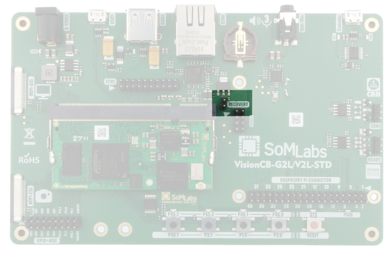
== RECOVERY jumper == | |||
[[File:VisionCB-x2L-STD-recovery.png|800px|center]] | |||
== Dimensions == | == Dimensions == | ||
[[File:VisionCB-x2L-STD-dimensions.png|800px|center]] | [[File:VisionCB-x2L-STD-dimensions.png|800px|center]] | ||
Latest revision as of 10:14, 4 January 2024

VisionCB-x2L-STD v.1.2 Datasheet and Pinout
General description
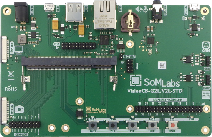
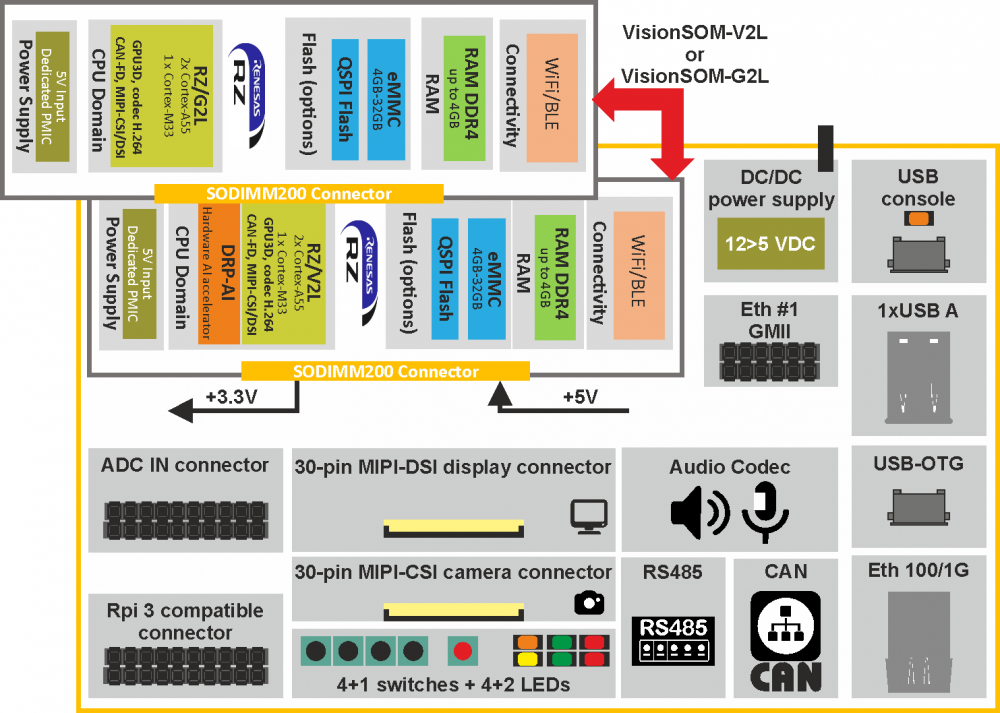
The VisionCB-x2L-STD (with SOM equipped with Renesas RZ/V2L and RZ/G2L MPUs compatible) is a carrier board for the VisionSOM-V2L and VisionSOM-G2L family of computer-on-modules which are powered by dual-core Renesas MPUs (2 x ARM Cortex-A55 + Cortex-M33). The carrier board, together with a System on Module (SoM), makes a complete development platform similar to SBC. The carrier board houses the most common interfaces such as USB, Ethernet, CAN, RS485, audio codec, etc. A large variety of interfaces allows to use it as both a complete development platform or as a stand-alone end-product. The VisionCB-x2L-STD is equipped with a simple user interface consisting of 4 buttons and 4 LEDs. VisionCB-x2L-STD carrier board is also equipped with a large number of popular peripherals, including: RS485, CAN, 10/100/1G Ethernet, MIPI display and camera connectors, serial console port on USB vCOM.
Applications
- Multimedia
- Video streaming
- Image inspection
- VisionAI gateway
- Doorbell systems
- EV chargers
- Smart agriculture gateways
- Industrial embedded Linux computer
- Home Appliances
- Home Automation – Smart Home
- Human-machine Interfaces (HMI)
- Point-of-sales (POS) terminals
- IoT gateways
- Machine vision equipment
- Robotics
- Fitness/outdoor equipment
Features
- Carrier Board compatible with the VisionSOM-G2L and VisionSOM-V2L families of modules based on dual core, heterogenous Renesas RZ/V2L and RZ/G2L application processors
- SoM Connector: SODIMM200
- Expansion Connectors:
- ADC+GPIO connector 2x9 Pin Header (Male)
- Raspberry Pi Compatible Connectors 2x20 Pin Header (Male)
- Ethernet #1 (GMII) Connector Pin Header (Male)
- Communication Connectors:
- 1x Ethernet 10/100/1000Mbit/s (RJ45)
- 1x CAN (1x3 Pin Header, Male)
- 1x RS-485 (1x3 Pin Header, Male)
- 1x USB Host Type A connectors
- 1x USB OTG Micro AB connector
- 1x Console MicroUSB B connector
- Audio Interface:
- Mini-jack 3.5mm (headphones + microphone)
- Display Interface:
- 30-pin FFC/FPC MIPI-DSI (up to 4 lanes)
- Camera Interface:
- 30-pin FFC/FPC MIPI-CSI2 (up to 4 lanes)
- User Interface:
- 4+1 Pushbuttons
- 4+2 LEDs
- External Power Supply 9-12V DC
- Temperature Range: 0 to +70°C
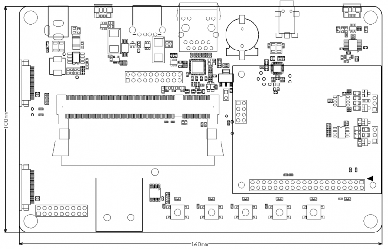
- Board Size: 160mm x 100mm x 21mm
Pictures of VisionCB-x2L-STD v1.2 board
| Version | Photo |
|---|---|
| VisionCB-x2L-STD v1.2 board only |
 |
| VisionCB-x2L-STD v1.2 with VisionSOM-x2L |
 |
Ordering info
Block Diagram
Electrical parameters
| Parameter | Value | Units | Comment | ||
|---|---|---|---|---|---|
| Min. | Typ. | Max. | |||
| Power Supply | 9.0 | 12.0 | 15.0 | V | Positive pole on central connector of J200 |
| Supply current | - | - | 0.13 | A | Excluding LCD, USB and antoher external loads |
| LCD/Camera Power Supply (logic) |
3.25 | 3.3 | 3.35 | V | - |
| LCD/Camera Power Supply (backlight and aux) |
4.75 | 4.87 | 4.95 | V | - |
| Arduino GPIO voltage | 3.3 | V | - | ||
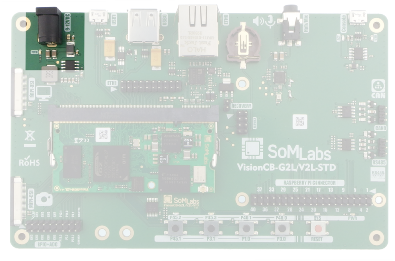
Power supply connector
The VisionCB-x2L-STD is equipped with external power source connector with pin diameter 2.5mm and hole diameter 6mm. The voltage of the external power source should be within the range 9-12 VDC.
Camera MIPI-CSI interface (FPC/FFC30, 0.5mm)
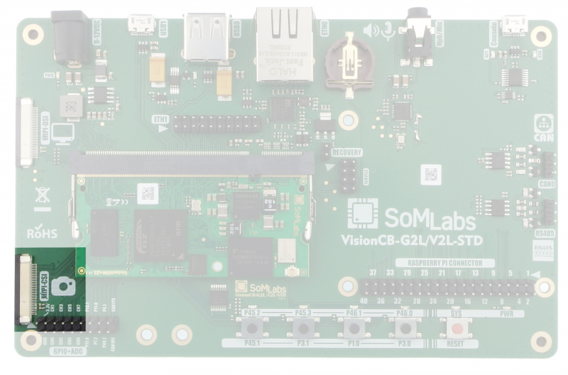
| Pin | Signal | GPIO | Description |
|---|---|---|---|
| 1 | GND | - | - |
| 2 | CSI-CLK-P | - | - |
| 3 | CSI-CLK-P | - | - |
| 4 | GND | - | - |
| 5 | CSI-DATA0-P | - | - |
| 6 | CSI-DATA0-N | - | - |
| 7 | GND | - | - |
| 8 | CSI-DATA1-P | - | - |
| 9 | CSI-DATA1-N | - | - |
| 10 | GND | - | - |
| 11 | CSI-DATA2-P | - | - |
| 12 | CSI-DATA2-N | - | - |
| 13 | GND | - | - |
| 14 | CSI-DATA3-P | - | - |
| 15 | CSI-DATA3-N | - | - |
| 16 | GND | - | - |
| 17 | I2C1-SCL | RIIC1_SCL | Camera confguration I2C interface (3.3V), pull-uped with 2.2k |
| 18 | I2C1-SDA | RIIC1_SDA | Camera confguration I2C interface (3.3V), pull-uped with 2.2k |
| 19 | GND | - | - |
| 20 | CSI-GPIO0 | P17-0 | Auxiliary GPIO |
| 21 | CSI-GPIO1 | P17-1 | Auxiliary GPIO |
| 22 | - | - | - |
| 23 | GND | - | - |
| 24 | +3.3V | - | Power supply for external devices |
| 25 | +3.3V | - | Power supply for external devices |
| 26 | +5V | - | Power supply for external devices |
| 27 | +5V | - | Power supply for external devices |
| 28 | - | - | - |
| 29 | - | - | - |
| 30 | GND | - | - |
Note:
1. The first pin of the MIPI-CSI connector is located in its upper part.
Display MIPI-DSI interface (FPC/FFC30, 0.5mm)
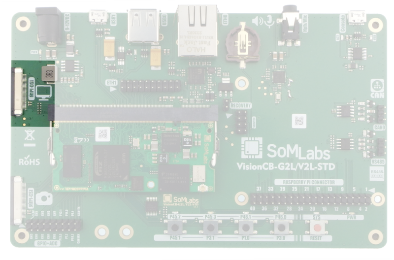
| Pin | Signal | GPIO | Description |
|---|---|---|---|
| 1 | GND | - | |
| 2 | DSI-CLK-P | - | - |
| 3 | DSI-CLK-P | - | - |
| 4 | GND | - | - |
| 5 | DSI-DATA0-P | - | - |
| 6 | DSI-DATA0-N | - | - |
| 7 | GND | - | - |
| 8 | DSI-DATA1-P | - | - |
| 9 | DSI-DATA1-N | - | - |
| 10 | GND | - | - |
| 11 | DSI-DATA2-P | - | - |
| 12 | DSI-DATA2-N | - | - |
| 13 | GND | - | - |
| 14 | DSI-DATA3-P | - | - |
| 15 | DSI-DATA3-N | - | - |
| 16 | GND | - | - |
| 17 | I2C1-SCL | RIIC1_SCL | Display confguration I2C interface (3.3V), pull-uped with 2.2k |
| 18 | I2C1-SDA | RIIC1_SDA | Display confguration I2C interface (3.3V), pull-uped with 2.2k |
| 19 | GND | - | - |
| 20 | DISP-RST | P13-2 | Optional display reset signal |
| 21 | TP-INT | P17-1 | Optional touch-panel interrupt signal |
| 22 | TP-RST | P17-2 | Optional touch-panel reset signal |
| 23 | GND | - | - |
| 24 | +3.3V | - | Power supply for external devices |
| 25 | +3.3V | - | Power supply for external devices |
| 26 | +5V | - | Power supply for external devices |
| 27 | +5V | - | Power supply for external devices |
| 28 | DSI-BL-PWM | P16-0 | Optional PWM backlight signal |
| 29 | DSI-BL-EN | P16-1 | Optional ENABLE backlight signal |
| 30 | GND | - | - |
Note:
1. The first pin of the MIPI-DSI connector is located in its upper part.
USB Console Port
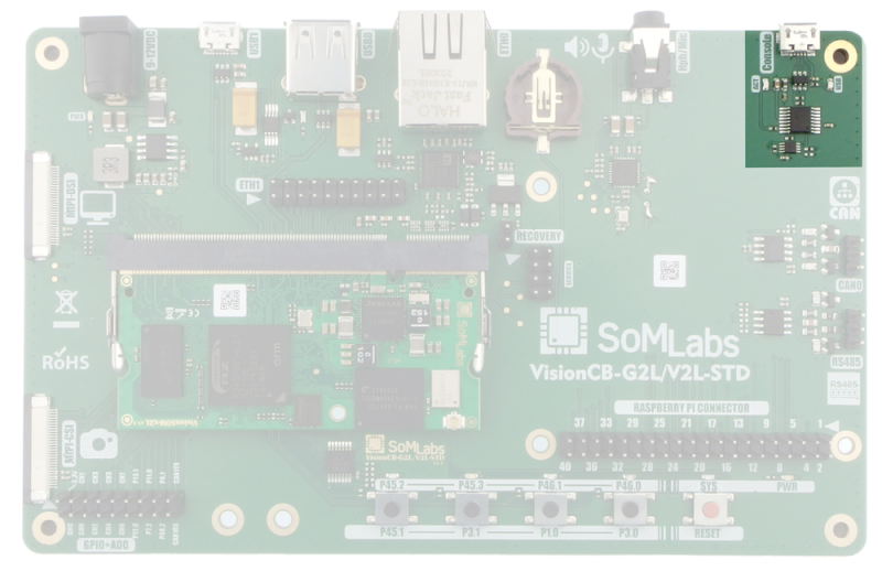
| Console line | MPU signal | GPIO | Description |
|---|---|---|---|
| CONSOLE-TXD | UART0-RXD | P38-1 | GPIO 3.3V voltage levels |
| CONSOLE-RXD | UART0-TXD | P38-0 | GPIO 3.3V voltage levels |
ADC + GPIO connector
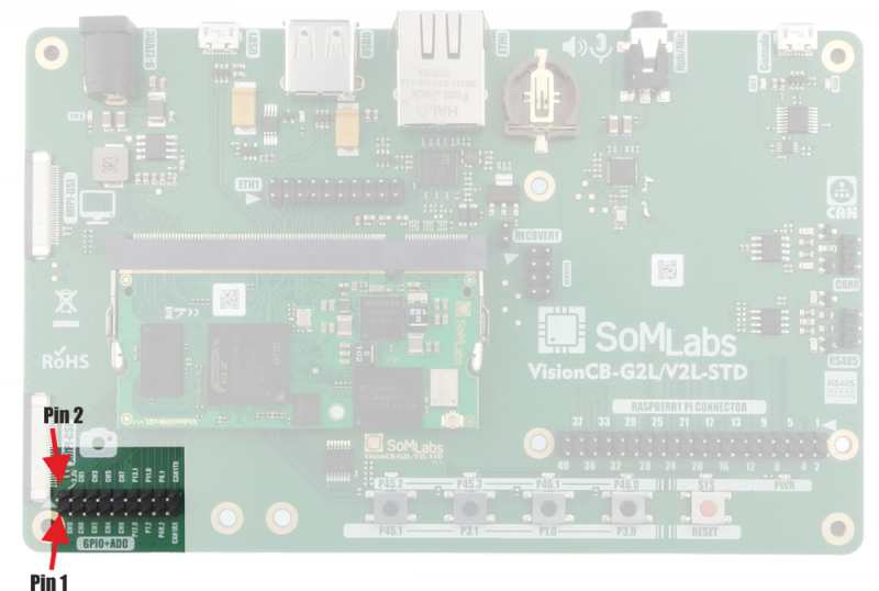
| Pin | Signal | GPIO | Description |
|---|---|---|---|
| 1 | GND | - | - |
| 2 | 3.3V | - | - |
| 3 | ADC-CH0 | ADC-CH0 | Dedicated analog input, 12-bit ADC, max. 1.8V on input |
| 4 | ADC-CH1 | ADC-CH1 | Dedicated analog input, 12-bit ADC, max. 1.8V on input |
| 5 | ADC-CH2 | ADC-CH2 | Dedicated analog input, 12-bit ADC, max. 1.8V on input |
| 6 | ADC-CH3 | ADC-CH3 | Dedicated analog input, 12-bit ADC, max. 1.8V on input |
| 7 | ADC-CH4 | ADC-CH4 | Dedicated analog input, 12-bit ADC, max. 1.8V on input |
| 8 | ADC-CH5 | ADC-CH5 | Dedicated analog input, 12-bit ADC, max. 1.8V on input |
| 9 | ADC-CH6 | ADC-CH6 | Dedicated analog input, 12-bit ADC, max. 1.8V on input |
| 10 | ADC-CH7 | ADC-CH7 | Dedicated analog input, 12-bit ADC, max. 1.8V on input |
| 11 | P12-0 | P12-0 | GPIO 3.3V voltage levels |
| 12 | P13-1 | P13-1 | GPIO 3.3V voltage levels |
| 13 | P7-2 | P7-2 | GPIO 3.3V voltage levels |
| 14 | P11-0 | P11-0 | GPIO 3.3V voltage levels |
| 15 | P48-2 | P48-2 | GPIO 3.3V voltage levels |
| 16 | P4-1 | P4-1 | GPIO 3.3V voltage levels |
| 17 | CAN1-RX | P13-0 | GPIO 3.3V voltage levels |
| 18 | CAN1-TX | P12-1 | GPIO 3.3V voltage levels |
Raspberry Pi compatible I/O header
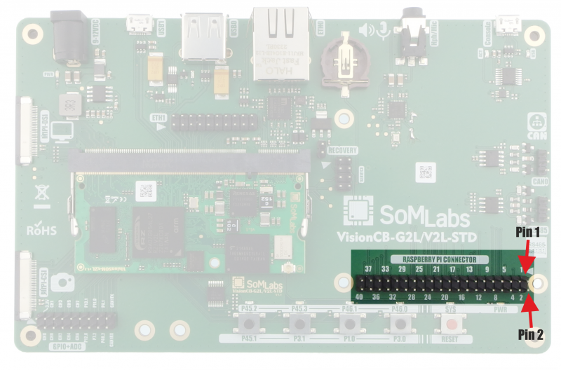
| Pin | Signal | MPU signal | Description |
|---|---|---|---|
| 1 | 3.3V | - | - |
| 2 | 5.0V | - | - |
| 3 | I2C0-SDA | RIIC0_SDA | Dedicated I2C MPU line |
| 4 | 5.0V | - | - |
| 5 | I2C0-SCL | RIIC0_SCL | Dedicated I2C MPU line |
| 6 | GND | - | - |
| 7 | P45-0 | P45-0 | GPIO 3.3V voltage levels |
| 8 | UART4-TXD | P2-0 | GPIO 3.3V voltage levels |
| 9 | GND | - | - |
| 10 | UART4-RXD | P2-1 | GPIO 3.3V voltage levels |
| 11 | P8-2 | P8-2 | GPIO 3.3V voltage levels |
| 12 | P15-0 | P15-0 | GPIO 3.3V voltage levels |
| 13 | P14-1 | P14-1 | GPIO 3.3V voltage levels |
| 14 | GND | - | - |
| 15 | P14-0 | P14-0 | GPIO 3.3V voltage levels |
| 16 | UART1-RXD | P40-0 | GPIO 3.3V voltage levels |
| 17 | P11-1 | P11-1 | GPIO 3.3V voltage levels |
| 18 | UART1-TXD | P40-1 | GPIO 3.3V voltage levels |
| 19 | SPI0-MOSI | P43-1 | GPIO 3.3V voltage levels |
| 20 | GND | - | - |
| 21 | SPI0-MISO | P43-2 | GPIO 3.3V voltage levels |
| 22 | P9-1 | P9-1 | GPIO 3.3V voltage levels |
| 23 | SPI0-CLK | P43-0 | GPIO 3.3V voltage levels |
| 24 | SPI0-SSL | P43-3 | GPIO 3.3V voltage levels |
| 25 | GND | - | - |
| 26 | P9-0 | P9-0 | GPIO 3.3V voltage levels |
| 27 | I2C3-SDA | P46-2 | I2C interface used by MPU for SOM PMIC configuration |
| 28 | I2C3-SCL | P46-3 | I2C interface used by MPU for SOM PMIC configuration |
| 29 | UART1-CTS | P41-0 | GPIO 3.3V voltage levels |
| 30 | GND | - | - |
| 31 | UART1-RTS | P41-1 | GPIO 3.3V voltage levels |
| 32 | P1-1 | P1-1 | GPIO 3.3V voltage levels |
| 33 | P10-1 | P10-1 | GPIO 3.3V voltage levels |
| 34 | GND | - | - |
| 35 | SPI1-MISO | P44-2 | GPIO 3.3V voltage levels |
| 36 | SPI1-SSL | P44-3 | GPIO 3.3V voltage levels |
| 37 | P10-0 | P10-0 | GPIO 3.3V voltage levels |
| 38 | SPI1-MOSI | P44-1 | GPIO 3.3V voltage levels |
| 39 | GND | - | - |
| 40 | SPI1-CLK | P44-0 | GPIO 3.3V voltage levels |
GMII of ETH0 connection
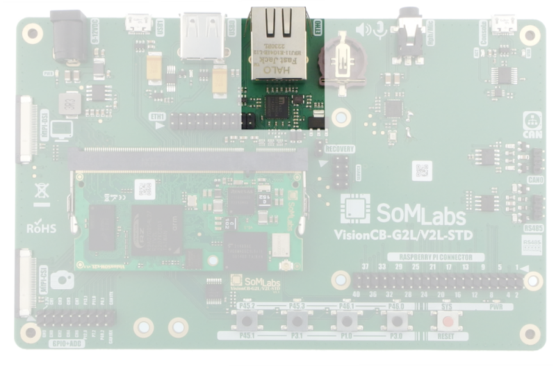
| Signal | MPU signal | Description |
|---|---|---|
| ET0-TXD0 | ET0-TXD0 | 1.8V Power Domain, GPIO mode not allowed |
| ET0-TXD1 | ET0-TXD1 | 1.8V Power Domain, GPIO mode not allowed |
| ET0-TXD2 | ET0-TXD2 | 1.8V Power Domain, GPIO mode not allowed |
| ET0-TXD3 | ET0-TXD3 | 1.8V Power Domain, GPIO mode not allowed |
| ET0-TXC | ET0-TXC | 1.8V Power Domain, GPIO mode not allowed |
| ET0-TX-CTL | ET0-TX-CTL | 1.8V Power Domain, GPIO mode not allowed |
| ET0-RXD0 | ET0-RXD0 | 1.8V Power Domain, GPIO mode not allowed |
| ET0-RXD1 | ET0-RXD1 | 1.8V Power Domain, GPIO mode not allowed |
| ET0-RXD2 | ET0-RXD2 | 1.8V Power Domain, GPIO mode not allowed |
| ET0-RXD3 | ET0-RXD3 | 1.8V Power Domain, GPIO mode not allowed |
| ET0-RXC | ET0-RXC | 1.8V Power Domain, GPIO mode not allowed |
| ET0-RX-CTL | ET0-RX-CTL | 1.8V Power Domain, GPIO mode not allowed |
| ET0-MDC | ET0-MDC | 1.8V Power Domain, GPIO mode not allowed |
| ET0-MDIO | ET0-MDIO | 1.8V Power Domain, GPIO mode not allowed |
| ET0-INT | P47-0 | GPIO 3.3V voltage levels |
| ET0-PHY-RST | P47-1 | GPIO 3.3V voltage levels |
GMII of ETH1 connector
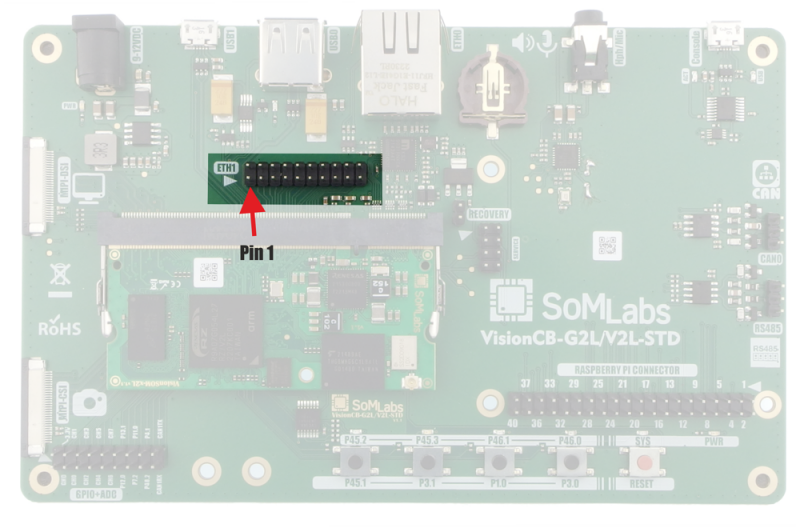
| Pin | Signal | MPU signal | Description |
|---|---|---|---|
| 1 | 3.3V | - | - |
| 2 | ET1-TXD0 | P30-0 | 1.8V or 3.3V Power Domain selected by ET1-VDD-SEL, GPIO allowed only for 3.3V. |
| 3 | ET1-TXD1 | P30-1 | 1.8V or 3.3V Power Domain selected by ET1-VDD-SEL, GPIO allowed only for 3.3V. |
| 4 | ET1-TXD2 | P31-0 | 1.8V or 3.3V Power Domain selected by ET1-VDD-SEL, GPIO allowed only for 3.3V. |
| 5 | ET1-TXD3 | P31-1 | 1.8V or 3.3V Power Domain selected by ET1-VDD-SEL, GPIO allowed only for 3.3V. |
| 6 | ET1-TXC | P29-0 | 1.8V or 3.3V Power Domain selected by ET1-VDD-SEL, GPIO allowed only for 3.3V. |
| 7 | ET1-TX-CTL | P29-1 | 1.8V or 3.3V Power Domain selected by ET1-VDD-SEL, GPIO allowed only for 3.3V. |
| 8 | ET1-RXD3 | P36-0 | 1.8V or 3.3V Power Domain selected by ET1-VDD-SEL, GPIO allowed only for 3.3V. |
| 9 | ET1-RXD2 | P35-1 | 1.8V or 3.3V Power Domain selected by ET1-VDD-SEL, GPIO allowed only for 3.3V. |
| 10 | ET1-RXD1 | P35-0 | 1.8V or 3.3V Power Domain selected by ET1-VDD-SEL, GPIO allowed only for 3.3V. |
| 11 | ET1-RXD0 | P34-1 | 1.8V or 3.3V Power Domain selected by ET1-VDD-SEL, GPIO allowed only for 3.3V. |
| 12 | ET1-RX-CTL | P34-0 | 1.8V or 3.3V Power Domain selected by ET1-VDD-SEL, GPIO allowed only for 3.3V. |
| 13 | ET1-RXC | P33-1 | 1.8V or 3.3V Power Domain selected by ET1-VDD-SEL, GPIO allowed only for 3.3V. |
| 14 | ET1-MDC | P37-0 | 1.8V or 3.3V Power Domain selected by ET1-VDD-SEL, GPIO allowed only for 3.3V. |
| 15 | ET1-MDIO | P37-1 | 1.8V or 3.3V Power Domain selected by ET1-VDD-SEL, GPIO allowed only for 3.3V. |
| 16 | ET1-INT | P47-2 | 1.8V or 3.3V Power Domain selected by ET1-VDD-SEL, GPIO allowed only for 3.3V. |
| 17 | ET1-PHY-RST | P47-3 | 1.8V or 3.3V Power Domain selected by ET1-VDD-SEL, GPIO allowed only for 3.3V. |
| 18 | ET1-VDD-SEL | - | Ethernet 1 (ET1) interface voltage selection: ET1-VDD-SEL='0' -> V=1.8V; ET1-VDD-SEL='1' or left open -> V=3.3V The line has internal pull-up. |
| 19 | GND | - | - |
| 20 | GND | - | - |
USB interfaces
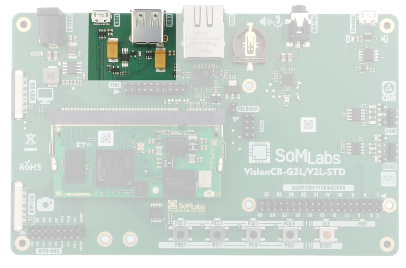
| Signal | MPU signal | Description |
|---|---|---|
| USB0-ID | P5-1 | GPIO 3.3V voltage levels |
| USB0-EN | P4-0 | GPIO 3.3V voltage levels |
| USB0-OC | P5-0 | GPIO 3.3V voltage levels |
| USB1-EN | P8-0 | GPIO 3.3V voltage levels |
| USB1-OC | P8-1 | GPIO 3.3V voltage levels |
Note:
1. USB0 is configured as host, USB1 channel is configured as USB-OTG.
Audio codec
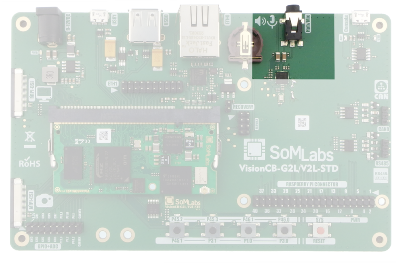
| Signal | MPU signal | Description |
|---|---|---|
| SSI-MCLK | AUDIO_CLK1 | GPIO 3.3V voltage levels |
| SSI0-BCK | P6-0 | GPIO 3.3V voltage levels |
| SSI0-RCK | P6-1 | GPIO 3.3V voltage levels |
| SSI0-TXD | P7-0 | GPIO 3.3V voltage levels |
| SSI0-RXD | P7-1 | GPIO 3.3V voltage levels |
Note:
1. Audio codec is configured via I2C2 MPU interface.
CAN interface
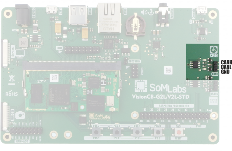
| Signal | MPU signal | Description |
|---|---|---|
| CAN0-RX | P42-2 | GPIO 3.3V voltage levels |
| CAN0-TX | P42-1 | GPIO 3.3V voltage levels |
| CAN0-STB | P18-1 | GPIO 3.3V voltage levels (STB line of MCP2542FD) |
RS-485 interface
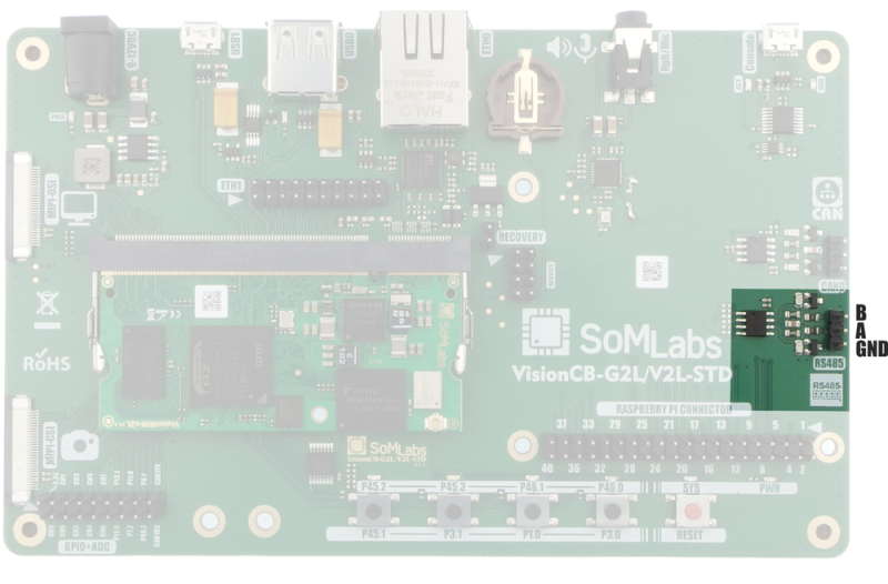
| Signal | MPU signal | Description |
|---|---|---|
| UART3-RXD | P0-1 | GPIO 3.3V voltage levels |
| UART3-TXD | P0-0 | GPIO 3.3V voltage levels |
| RS485-RE | P18-0 | GPIO 3.3V voltage levels In default configuration RS485-RE is connected to nRE and DE inputs of MAX3485 |
| RS485-DE | P19-0 | GPIO 3.3V voltage levels In default configuration this line is not used |
User Interface (switches and LEDs)
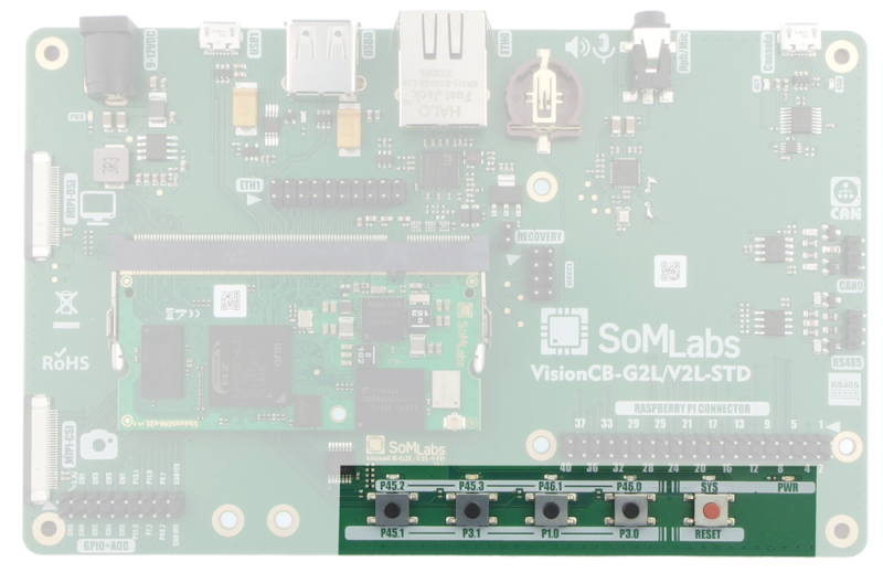
| Signal | MPU signal | Description |
|---|---|---|
| User LEDs | ||
| P45-2 | P45-2 | Inverted logic level |
| P45-3 | P45-3 | Inverted logic level |
| P46-0 | P46-0 | Inverted logic level |
| P46-1 | P46-1 | Inverted logic level |
| SYS-LED | P42-0 | Inverted logic level |
| User switch | ||
| P1-0 | P1-0 | Pushbutton, line pull-uped |
| P3-0 | P3-0 | Pushbutton, line pull-uped |
| P3-1 | P3-1 | Pushbutton, line pull-uped |
| P45-1 | P45-1 | Pushbutton, line pull-uped |
RECOVERY jumper
Dimensions
