VisionCB-RT1176-STD v.1.2 Datasheet and Pinout: Difference between revisions
From SomLabs Wiki
| (22 intermediate revisions by the same user not shown) | |||
| Line 10: | Line 10: | ||
=== Applications === | === Applications === | ||
* | * Industrial embedded RTOS computer | ||
* Home | * Home Appliances | ||
* Air Conditioning | |||
* Building Security | |||
* Fleet Management | |||
* Heat Metering | |||
* Home Automation – Smart Home | * Home Automation – Smart Home | ||
* Human-machine Interfaces (HMI) | * Human-machine Interfaces (HMI) | ||
* Motor Drives | * Motor Drives | ||
* | * Cash Register | ||
* Smart grid | * Intermediate Flight Controller | ||
* Smart grid Infrastructure | |||
* IoT gateways | * IoT gateways | ||
* | * Residential getaways | ||
* | * Smart Lock | ||
* | * Robotics | ||
* | * Toys and Board Games | ||
== Features == | == Features == | ||
| Line 311: | Line 315: | ||
| I2C1.SDA | | I2C1.SDA | ||
| GPIO_AD_33 | | GPIO_AD_33 | ||
| | | 4,7kOhm pull-up resistor | ||
|- | |- | ||
| 6 | | 6 | ||
| I2C1.SCL | | I2C1.SCL | ||
| GPIO_AD_32 | | GPIO_AD_32 | ||
| | | 4,7kOhm pull-up resistor | ||
|- | |- | ||
| 7 | | 7 | ||
| I2C2.SDA | | I2C2.SDA | ||
| GPIO_AD_19 | | GPIO_AD_19 | ||
| | | 4,7kOhm pull-up resistor | ||
|- | |- | ||
| 8 | | 8 | ||
| I2C2.SCL | | I2C2.SCL | ||
| GPIO_AD_18 | | GPIO_AD_18 | ||
| | | 4,7kOhm pull-up resistor | ||
|- | |- | ||
| 9 | | 9 | ||
| Line 371: | Line 375: | ||
Notes:<br /> | Notes:<br /> | ||
1. NA - not available.<br /> | 1. NA - not available.<br /> | ||
== GPIO COMM2 I/O header (J801) == | == GPIO COMM2 I/O header (J801) == | ||
| Line 564: | Line 567: | ||
Notes:<br /> | Notes:<br /> | ||
1. NA - not available.<br /> | 1. NA - not available.<br /> | ||
== Audio codec == | |||
[[File:VisionCB-RT1176-STD-AUDIO.png|center|600px]] | |||
{| class="wikitable" | |||
! style="text-align: center; font-weight: bold;" | PCB designation | |||
! style="text-align: center; font-weight: bold;" | MCU pin name | |||
! style="text-align: center; font-weight: bold;" | Description | |||
|- | |||
| SAI1.MCLK | |||
| GPIO_DISP_B2_03 | |||
| Audio interface MCLK signal | |||
|- | |||
| SAI1.BCLK | |||
| GPIO_DISP_B2_05 | |||
| Audio interface BCLK signal | |||
|- | |||
| SAI1.FSYNC | |||
| GPIO_DISP_B2_04 | |||
| Audio interface FSYNC signal | |||
|- | |||
| SAI1.TX | |||
| GPIO_DISP_B2_07 | |||
| Audio interface TX signal | |||
|- | |||
| SAI1.RX | |||
| GPIO_DISP_B2_06 | |||
| Audio interface TX signal | |||
|- | |||
| I2C5.SCL | |||
| GPIO_LPSR_09 | |||
| Codec configuration SCL line of I2C5 interface<br>4,7kOhm pull-up resistor | |||
|- | |||
| I2C5.SDA | |||
| GPIO_LPSR_08 | |||
| Codec configuration SDA line of I2C5 interface<br>4,7kOhm pull-up resistor | |||
|} | |||
== USB-OTG == | |||
[[File:VisionCB-RT1176-STD-USBOTG.png|center|600px]] | |||
{| class="wikitable" | |||
! style="text-align: center; font-weight: bold;" | PCB designation | |||
! style="text-align: center; font-weight: bold;" | MCU pin name | |||
! style="text-align: center; font-weight: bold;" | Description | |||
|- | |||
| USB1.EN | |||
| GPIO_AD_12 | |||
| Power enable signal connected to USB power switch (STMPS2252). | |||
|- | |||
| USB1.OC | |||
| GPIO_AD_10 | |||
| Over-current signal input (from USB power switch STMPS2252). | |||
|- | |||
| USB1.ID | |||
| GPIO_AD_09 | |||
| USB device identification input. | |||
|} | |||
Notes:<br> | |||
1. USB-OTG is connected to USB1 interface of MCU.<br> | |||
2. D+/D-/VBUS signals are connected to dedicated analog MCU pins.<br> | |||
3. USB1.OC controls OverCurrent red LED (D300). | |||
== USB host == | |||
[[File:VisionCB-RT1176-STD-USBHOST.png|center|600px]] | |||
{| class="wikitable" | |||
! style="text-align: center; font-weight: bold;" | PCB designation | |||
! style="text-align: center; font-weight: bold;" | MCU pin name | |||
! style="text-align: center; font-weight: bold;" | Description | |||
|- | |||
| USB2.EN | |||
| GPIO_AD_12 | |||
| Power enable signal connected to USB power switch (STMPS2252). | |||
|- | |||
| USB2.OC | |||
| GPIO_AD_13 | |||
| Over-current signal input (from USB power switch STMPS2252). | |||
|} | |||
Notes:<br> | |||
1. USB Host is connected to USB2 interface of MCU.<br> | |||
2. D+/D-/VBUS signals are connected to dedicated analog MCU pins.<br> | |||
3. USB2.OC controls OverCurrent red LED (D300). | |||
== User LEDs connections == | == User LEDs connections == | ||
| Line 617: | Line 703: | ||
| JTAG.MOD input with internal pull-down by 10 kOhm resistor. | | JTAG.MOD input with internal pull-down by 10 kOhm resistor. | ||
|} | |} | ||
Notes:<br /> | |||
1. LED is switched on by logic „1” set at the GPIO outputs.<br /> | |||
2. LED is controlled by current drivers and do not load the GPIO.<br /> | |||
== User switches connections == | == User switches connections == | ||
| Line 708: | Line 797: | ||
== RS485 | == RS485 interface == | ||
[[File:VisionCB-RT1176-STD-RS485.png|center|600px]] | [[File:VisionCB-RT1176-STD-RS485.png|center|600px]] | ||
| Line 749: | Line 838: | ||
|} | |} | ||
== CAN | == CAN interface == | ||
[[File:VisionCB-RT1176-STD-CAN.png|center|600px]] | [[File:VisionCB-RT1176-STD-CAN.png|center|600px]] | ||
| Line 786: | Line 875: | ||
| GPIO3-21 | | GPIO3-21 | ||
| GPIO_AD_22 | | GPIO_AD_22 | ||
| Connected to STB input of CAN PHY (MCP2542FD) | | Connected to STB input of CAN PHY (MCP2542FD)<br>10kOhm pull-down resistor | ||
|} | |} | ||
| Line 1,135: | Line 1,224: | ||
== RTC/SNVS battery socket (J101) == | == RTC/SNVS battery socket (J101) == | ||
[[File:VisionCB-RT1176-STD-BATT.png|center|600px]] | [[File:VisionCB-RT1176-STD-BATT.png|center|600px]] | ||
Optional 3V cell (CR2032 or CR2025) for SNVS MCU backup power domain (VDD-COIN-3V). | |||
== Dimensions == | == Dimensions == | ||
[[File:VisionCB-RT1176-STD-v12-dimensions.png|800px|center]] | [[File:VisionCB-RT1176-STD-v12-dimensions.png|800px|center]] | ||
Latest revision as of 12:03, 9 July 2024

VisionCB-RT1176-STD v.1.2 Datasheet and Pinout
General description

VisionCB-RT1176-STD is a carrier board for the VisionSOM-RT1170 family of computer-on-modules, which are powered by NXP i.MX RT117x application processors. The carrier board, together with a System on Module (SoM), makes a complete development platform similar to SBC. The carrier board houses the most common interfaces such as audio codec, USB, Ethernet, UART, RS485, CAN etc. A large variety of interfaces allows to use it as both a complete development platform or as a stand-alone end-product.
The carrier board connects with the SoM via a standard SODIMM connector.
Applications
- Industrial embedded RTOS computer
- Home Appliances
- Air Conditioning
- Building Security
- Fleet Management
- Heat Metering
- Home Automation – Smart Home
- Human-machine Interfaces (HMI)
- Motor Drives
- Cash Register
- Intermediate Flight Controller
- Smart grid Infrastructure
- IoT gateways
- Residential getaways
- Smart Lock
- Robotics
- Toys and Board Games
Features
- Carrier Board (Base Board) compatible with the VisionSOM family of modules based on NXP i.MX RT117x application processors
- SoM connector: SODIMM200
- Expansion Connectors:
- GPIO-SNVS, GPIO-COMM1, GPIO-COMM2 2x16 Pin Headers (Male)
- MicroSD socket
- Audio:
- 24-bit codec audio with headphones and microphone Jack connector
- Communication Connectors:
- 1x JTAG connector
- RS485 half-duplex
- CAN single channel
- 1x Ethernet 10/100/1000 Mbit/s, RJ45
- 1x USB Host Type A connectors
- 1x USB-OTG Micro AB connector
- 1x Console MicroUSB B connector (Mbed SWDAP debug probe based on LPC11U35FHI33/501)
- Display Interface: 30-pin FFC/FPC MIPI-DSI
- Camera Interface: 30-pin FFC/FPC MIPI-CSI
- User Interface:
- 5 Pushbuttons
- 5 LEDs
- Recovery jumper
- Power Supply
- DC connector: Input Voltage 9-12V DC (5.5x2.1 connector)
- CR2032 battery socket for RTC
- Temperature Range: 0 to +70°C
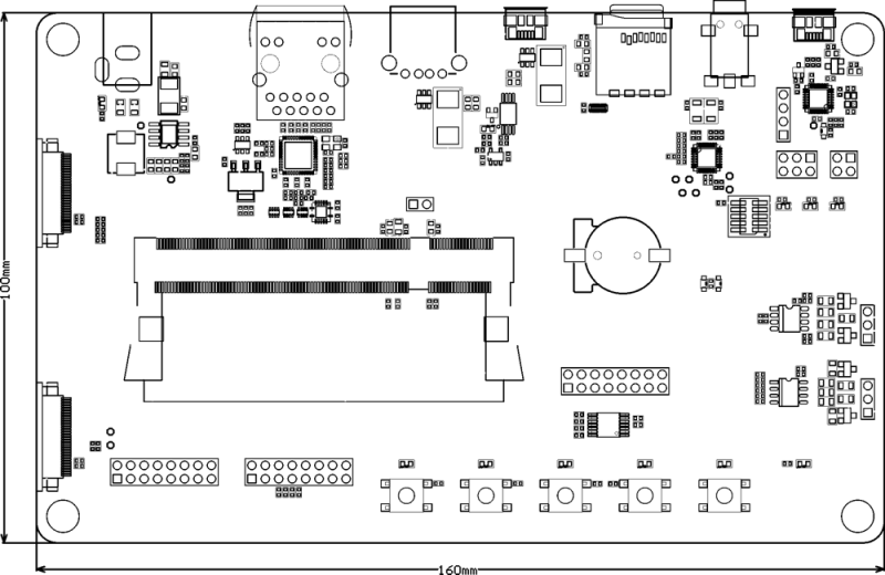
- Board Size: 160mm x 100mm x 22mm
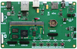
Pictures of VisionCB-RT1176-STD v1.2 board
| Version | Photo |
|---|---|
| VisionCB-RT1176-STD v1.2 board with attached SOM |
 |
Ordering info
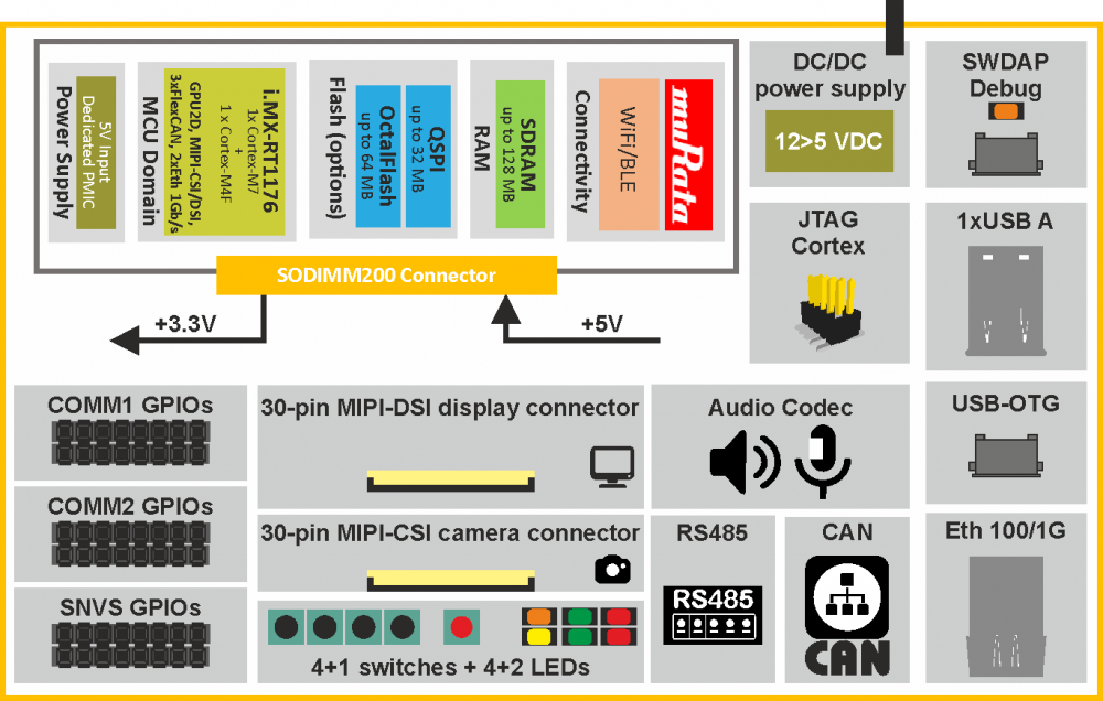
Block Diagram
Electrical parameters
| Parameter | Value | Units | Comment | ||
|---|---|---|---|---|---|
| Min. | Typ. | Max. | |||
| Power Supply (J100 input) | 9.0 | 12.0 | 15.0 | V | Positive pole on central connector of J200 |
| Supply current | - | - | 0.13 | A | Excluding LCD, USB and antoher external loads |
| Output voltage (VDD-3V3) | - | 3.3 | - | V | Generated by internal DC/DC converter on SoM |
| Output VDD-3V3 current | - | - | 80 | mA | Generated by internal DC/DC converter on SoM |
| Input GPIO COMM1/COMM2 voltage (J8011 and J802) | 0 | - | 3.3 | V | - |
| Input GPIO SNVS voltage (J800) | 0 | - | 1.8 | V | - |
| JTAG/SWD interface voltage (J900) | 0 | - | 3.3 | V | - |
| DAC output voltage range (J801) | 0 | - | 1.8 | V | - |
| MicroSD Card power supply voltage | - | - | 3.3 | V | - |
Note:
1. Excluding DAC output (pin 14 of J801, maximum allowable voltage 1.8V)
Recovery Jumper/MCU Boot Configuration
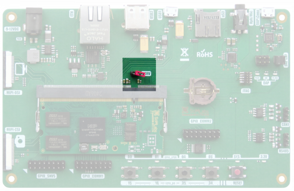
RECOVERY is the boot mode selector. If:
- RECOVERY = 0 (jupmer installed) then BOOT-MODE0 = 1, as a result serial loader starts
- RECOVERY = 1 (jumper is not installed) or open then BOOT-MODE0 = 0, as a result MCU boots from fuses
External JTAG Connector
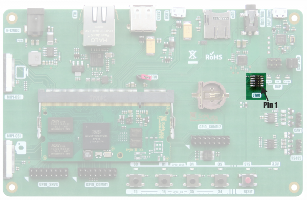
| JTAG Connector | Default function name | MCU pin name |
|---|---|---|
| 1 | +3V3 | - |
| 2 | TMS | GPIO_LPSR_15 |
| 3 | GND | NA |
| 4 | TCK | GPIO_LPSR_14 |
| 5 | GND | NA |
| 6 | TDO | GPIO_LPSR_11 |
| 7 | - | - |
| 8 | TDI | GPIO_LPSR_12 |
| 9 | GND | GPIO_AD_B0_07 |
| 10 | nRES/TRST | GPIO_LPSR_10 |
DAP Debug Interface
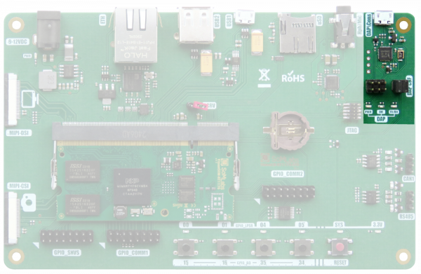
The DAP debug interface is based on LPC11U35FHI33/501 and converts USB into two-lines SWD debug interface.
The DAP debug interface also serves as an vCOM (on USB) interface for optional UART console port.
SWDIO DAP Connector
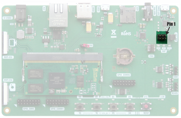
| DAP Connector | Function name | Source: DAP/SoM |
|---|---|---|
| 1 | nRES | DAP |
| 2 | nRESET | DAP |
| 3 | SWCLK | DAP |
| 4 | TCK | SoM |
| 5 | SWDIO | DAP |
| 6 | TMS | SoM |
Note:
1. During normal use, it is recommended to connect pin pairs: 1-2, 3-4, 5-6.
Console DAP Connector
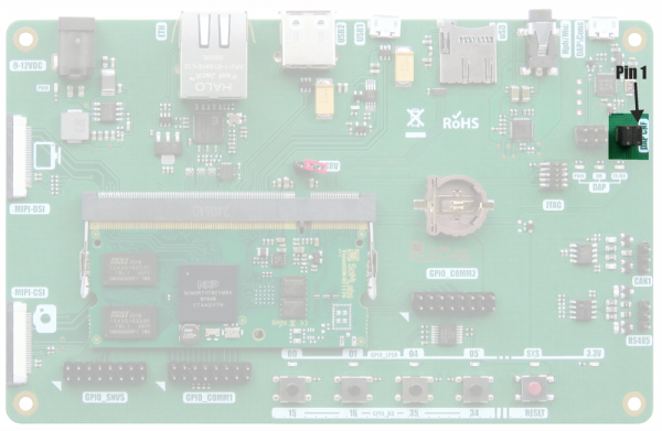
| DAP Connector | Function name | MCU pin name | Signal Source |
|---|---|---|---|
| 1 | RxD | - | DAP |
| 2 | UART2.RxD | GPIO_DISP_B2_11 | SoM |
| 3 | TxD | - | DAP |
| 4 | UART2.TxD | GPIO_DISP_B2_10 | SoM |
Note:
1. During normal use, it is recommended to connect pin pairs: 1-2, 3-4.
GPIO COMM1 I/O header (J802)
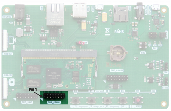
| J802 Pin | Default function name | MCU pin name | Description |
|---|---|---|---|
| 1 | SPI4.SCK | GPIO_DISP_B2_12 | 3.3V logic levels |
| 2 | SPI4.OUT | GPIO_DISP_B2_14 | 3.3V logic levels |
| 3 | SPI4.IN | GPIO_DISP_B2_13 | 3.3V logic levels |
| 4 | SPI4.CS0 | GPIO_DISP_B2_15 | 3.3V logic levels |
| 5 | I2C1.SDA | GPIO_AD_33 | 4,7kOhm pull-up resistor |
| 6 | I2C1.SCL | GPIO_AD_32 | 4,7kOhm pull-up resistor |
| 7 | I2C2.SDA | GPIO_AD_19 | 4,7kOhm pull-up resistor |
| 8 | I2C2.SCL | GPIO_AD_18 | 4,7kOhm pull-up resistor |
| 9 | CAN2.TX | GPIO_AD_00 | 3.3V logic levels |
| 10 | CAN2.RX | GPIO_AD_01 | 3.3V logic levels |
| 11 | UART1.RXD | GPIO_AD_25 | Available to the user as GPIO only in SoM without 1DX radio modules. |
| 12 | UART1.TXD | GPIO_AD_24 | Available to the user as GPIO only in SoM without 1DX radio modules. |
| 13 | UART1.CTS | GPIO_AD_26 | Available to the user as GPIO only in SoM without 1DX radio modules. |
| 14 | UART1.RTS | GPIO_AD_27 | Available to the user as GPIO only in SoM without 1DX radio modules. |
| 15 | +3V3 | NA | - |
| 16 | GND | NA | - |
Notes:
1. NA - not available.
GPIO COMM2 I/O header (J801)
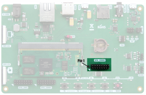
| J801 Pin | Default function name | MCU pin name | Description |
|---|---|---|---|
| 1 | UART5.TXD | GPIO_AD_28 | 3.3V logic levels |
| 2 | UART3.TXD | GPIO_AD_30 | 3.3V logic levels |
| 3 | UART5.RXD | GPIO_AD_29 | 3.3V logic levels |
| 4 | UART3.RXD | GPIO_AD_31 | 3.3V logic levels |
| 5 | UART10.TXD | GPIO_AD_15 | Pushbutton S804 is connected to this line. |
| 6 | UART12.TXD | GPIO_LPSR_00 | GPIO_LPSR00 LED is connected to this line (through logic inverter). |
| 7 | UART10.RXD | GPIO_AD_16 | Pushbutton S803 is connected to this line. |
| 8 | UART12.RXD | GPIO_LPSR_01 | GPIO_LPSR01 LED is connected to this line (through logic inverter). |
| 9 | UART10.RTS | GPIO_AD_35 | Pushbutton S802 is connected to this line. |
| 10 | UART12.RTS | GPIO_LPSR_04 | GPIO_LPSR04 LED is connected to this line (through logic inverter). |
| 11 | UART10.CTS | GPIO_AD_34 | Pushbutton S801 is connected to this line. |
| 12 | UART12.CTS | GPIO_LPSR_05 | GPIO_LPSR05 LED is connected to this line (through logic inverter). |
| 13 | NC | - | - |
| 14 | DAC-OUT | DAC-OUT | 12-bit DAC voltage output (range 0-1.8V). |
| 15 | +3V3 | NA | - |
| 16 | GND | NA | - |
Notes:
1. NA - not available.
2. NC - not connected.
GPIO SNVS I/O header (J800)
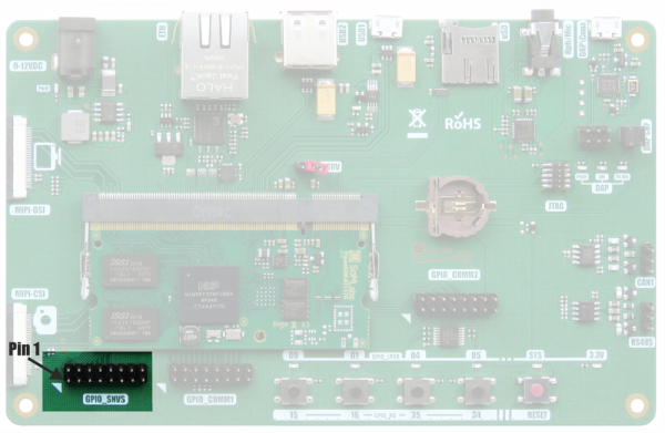
| J800 Pin | Default function name | MCU pin name | Description |
|---|---|---|---|
| 1 | GPIO-SVNS.9 | GPIO_SNVS_09 | 1.75V VDD_SNVS_ANA power domain |
| 2 | GPIO-SVNS.8 | GPIO_SNVS_08 | 1.75V VDD_SNVS_ANA power domain |
| 3 | GPIO-SVNS.7 | GPIO_SNVS_07 | 1.75V VDD_SNVS_ANA power domain |
| 4 | GPIO-SVNS.6 | GPIO_SNVS_06 | 1.75V VDD_SNVS_ANA power domain |
| 5 | GPIO-SVNS.5 | GPIO_SNVS_05 | 1.75V VDD_SNVS_ANA power domain |
| 6 | GPIO-SVNS.4 | GPIO_SNVS_04 | 1.75V VDD_SNVS_ANA power domain |
| 7 | GPIO-SVNS.3 | GPIO_SNVS_03 | 1.75V VDD_SNVS_ANA power domain |
| 8 | GPIO-SVNS.2 | GPIO_SNVS_02 | 1.75V VDD_SNVS_ANA power domain |
| 9 | GPIO-SVNS.1 | GPIO_SNVS_01 | 1.75V VDD_SNVS_ANA power domain |
| 10 | GPIO-SVNS.0 | GPIO_SNVS_00 | 1.75V VDD_SNVS_ANA power domain |
| 11 | PMIC-STBY-REQ | PMIC-STBY-REQ | 1.75V VDD_SNVS_ANA power domain. |
| 12 | RESET | RESET | POR-B of MCU line (resets all of the chip except the Secure Non-Volatile Storage (SNVS) block), active low. 1.75V VDD_SNVS_ANA power domain. |
| 13 | WAKEUP | - | A GPIO powered by SNVS domain power supply which can be configured as wakeup source in SNVS mode. 1.75V VDD_SNVS_ANA power domain. |
| 14 | ON-OFF | ON-OFF | A brief connection to GND in the OFF mode causes the internal power management state machine to change the state to ON. In the ON mode, a brief connection to GND generates an interrupt intended to be a software-controllable power-down). Approximately five seconds (or more) to GND causes a forced OFF. Both boot mode inputs can be disconnected. 1.75V VDD_SNVS_ANA power domain. |
| 15 | +1V8 | NA | Reference voltage for 1V8 peripherals. |
| 16 | GND | NA | - |
Notes:
1. NA - not available.
Audio codec
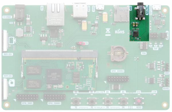
| PCB designation | MCU pin name | Description |
|---|---|---|
| SAI1.MCLK | GPIO_DISP_B2_03 | Audio interface MCLK signal |
| SAI1.BCLK | GPIO_DISP_B2_05 | Audio interface BCLK signal |
| SAI1.FSYNC | GPIO_DISP_B2_04 | Audio interface FSYNC signal |
| SAI1.TX | GPIO_DISP_B2_07 | Audio interface TX signal |
| SAI1.RX | GPIO_DISP_B2_06 | Audio interface TX signal |
| I2C5.SCL | GPIO_LPSR_09 | Codec configuration SCL line of I2C5 interface 4,7kOhm pull-up resistor |
| I2C5.SDA | GPIO_LPSR_08 | Codec configuration SDA line of I2C5 interface 4,7kOhm pull-up resistor |
USB-OTG
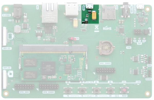
| PCB designation | MCU pin name | Description |
|---|---|---|
| USB1.EN | GPIO_AD_12 | Power enable signal connected to USB power switch (STMPS2252). |
| USB1.OC | GPIO_AD_10 | Over-current signal input (from USB power switch STMPS2252). |
| USB1.ID | GPIO_AD_09 | USB device identification input. |
Notes:
1. USB-OTG is connected to USB1 interface of MCU.
2. D+/D-/VBUS signals are connected to dedicated analog MCU pins.
3. USB1.OC controls OverCurrent red LED (D300).
USB host
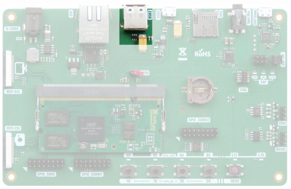
| PCB designation | MCU pin name | Description |
|---|---|---|
| USB2.EN | GPIO_AD_12 | Power enable signal connected to USB power switch (STMPS2252). |
| USB2.OC | GPIO_AD_13 | Over-current signal input (from USB power switch STMPS2252). |
Notes:
1. USB Host is connected to USB2 interface of MCU.
2. D+/D-/VBUS signals are connected to dedicated analog MCU pins.
3. USB2.OC controls OverCurrent red LED (D300).
User LEDs connections
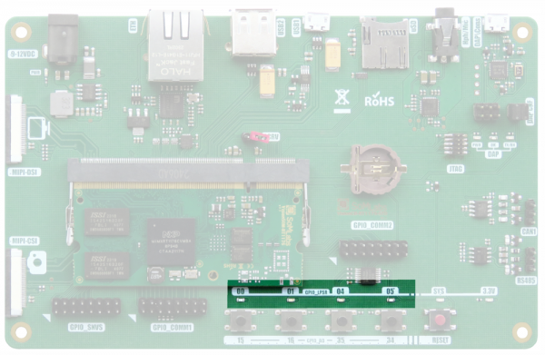
| LED | PCB designation | MCU pin name | Description |
|---|---|---|---|
| D804 | SYS | JTAG.MOD | JTAG.MOD input with internal pull-down by 10 kOhm resistor. |
| D803 | GPIO_LPSR_00 | UART12.TXD | Line connected to J801 (GPIO COMM2). |
| D802 | GPIO_LPSR_01 | UART12.RXD | Line connected to J801 (GPIO COMM2). |
| D801 | GPIO_LPSR_04 | UART12.RTS | Line connected to J801 (GPIO COMM2). |
| D800 | GPIO_LPSR_05 | UART12.CTS | Line connected to J801 (GPIO COMM2). |
Notes:
1. LEDs are switched on by logic „1” set at the GPIO outputs.
2. LEDs are controlled by current drivers and do not load the GPIOs.
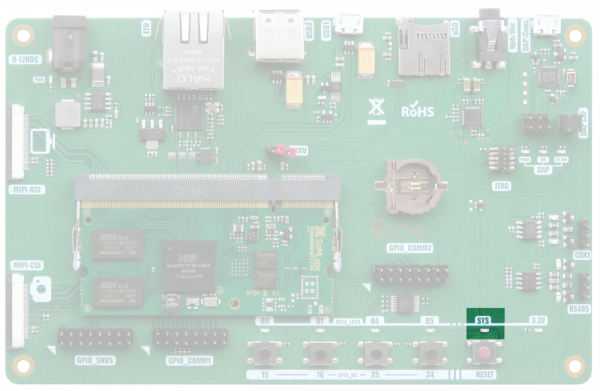
| LED | PCB designation | MCU pin name | Description |
|---|---|---|---|
| D804 | SYS | JTAG.MOD | JTAG.MOD input with internal pull-down by 10 kOhm resistor. |
Notes:
1. LED is switched on by logic „1” set at the GPIO outputs.
2. LED is controlled by current drivers and do not load the GPIO.
User switches connections
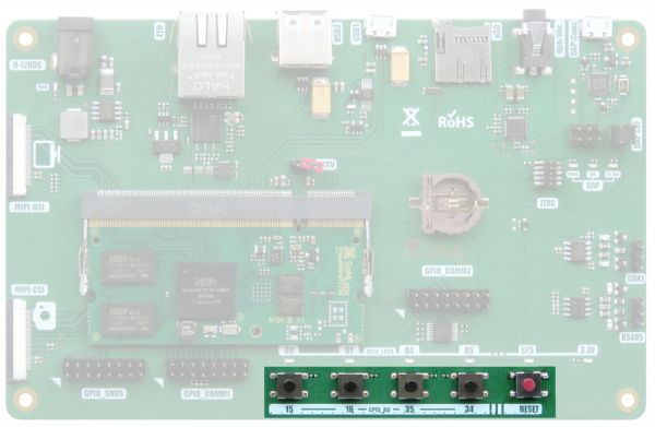
| Switch | PCB designation | MCU pin name | Description |
|---|---|---|---|
| S804 | UART10.TXD | GPIO_AD_15 | Line connected to J801 (GPIO COMM2) connector. |
| S803 | UART10.RXD | GPIO_AD_16 | Line connected to J801 (GPIO COMM2) connector. |
| S802 | UART10.RTS | GPIO_AD_35 | Line connected to J801 (GPIO COMM2) connector. |
| S801 | UART10.CTS | GPIO_AD_34 | Line connected to J801 (GPIO COMM2) connector. |
Notes:
1. After button pressing on GPIO lines are set to „0”.
2. GPIO lines connected to switches are separated from board’s environment by 100R resistors.
3. The function of red pushbutton is main system reset (connected to RESET-IN SoM input).
MicroSD card socket
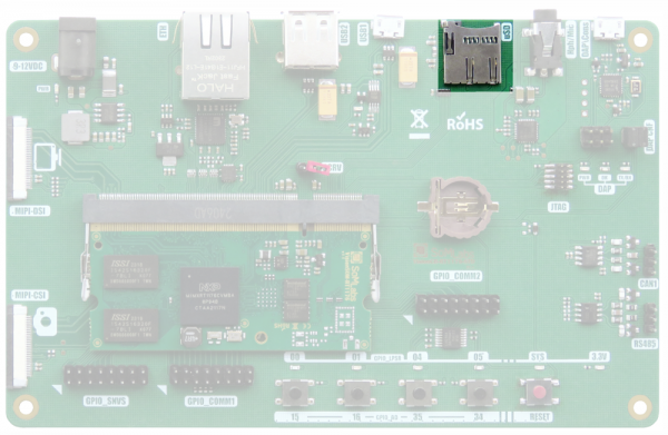
| Socket pin | PCB designation | MCU pin name | Description |
|---|---|---|---|
| 1 | SD1.DATA2 | GPIO_SD_B1_04 | Available to the user as GPIO only in modules without 1DX radio modules |
| 2 | SD1.DATA3 | GPIO_SD_B1_05 | Available to the user as GPIO only in modules without 1DX radio modules |
| 3 | SD1.CMD | GPIO_SD_B1_00 | Available to the user as GPIO only in modules without 1DX radio modules |
| 4 | VDD (3V3) | - | - |
| 5 | SD1.CLK | GPIO_SD_B1_01 | Available to the user as GPIO only in modules without 1DX radio modules |
| 6 | GND | - | - |
| 7 | SD1.DATA0 | GPIO_SD_B1_02 | Available to the user as GPIO only in modules without 1DX radio modules |
| 8 | SD1.DATA1 | GPIO_SD_B1_03 | Available to the user as GPIO only in modules without 1DX radio modules |
RS485 interface
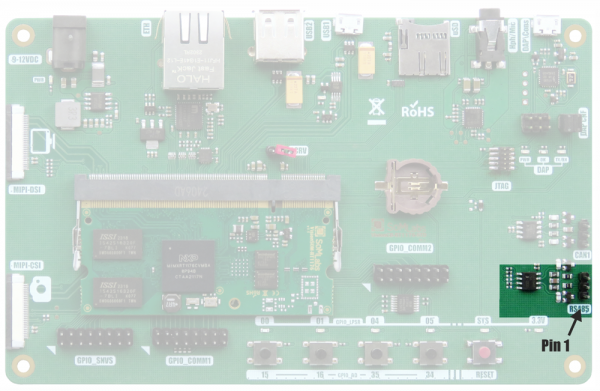
| Pin connector (J701) | PCB designation | Description |
|---|---|---|
| 1 | GND | - |
| 2 | A | RS485 transceiver "A" line (half-duplex interface) |
| 3 | B | RS485 transceiver "B" line (half-duplex interface) |
| PCB designation | MCU pin | Description |
|---|---|---|
| UART8.RXD | GPIO_AD_03 | MCU UART input from RS485 PHY transceiver |
| UART8.TXD | GPIO_AD_02 | MCU UART output to RS485 PHY transceiver |
| UART8.RTS | GPIO_AD_05 | Connected to nRE and DE pins of RS485 PHY transceiver |
CAN interface
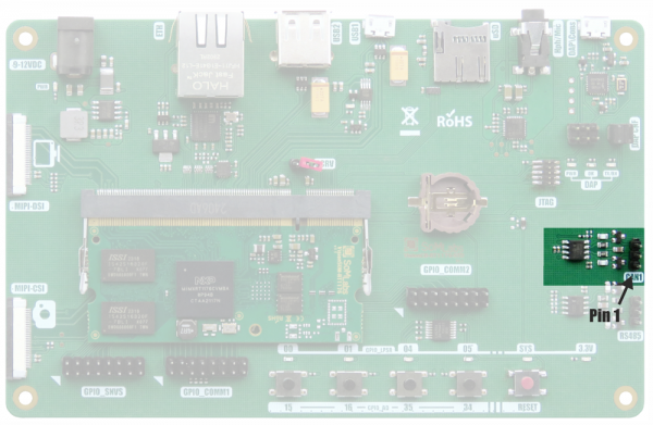
| Pin connector (J700) | PCB designation | Description |
|---|---|---|
| 1 | GND | - |
| 2 | CANL | CAN transceiver L data line |
| 3 | CANH | CAN transceiver H data line |
| PCB designation | MCU pin | Description |
|---|---|---|
| CAN1.TX | GPIO_AD_06 | MCU CAN data output |
| CAN1.RX | GPIO_AD_07 | MCU CAN data intput |
| GPIO3-21 | GPIO_AD_22 | Connected to STB input of CAN PHY (MCP2542FD) 10kOhm pull-down resistor |
Ethernet socket
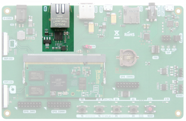
| PCB designation | MCU pin name | Description |
|---|---|---|
| ENET.RXD0 | GPIO_DISP_B1_02 | ENET-QOS.RXD0 |
| ENET.RXD1 | GPIO_DISP_B1_03 | ENET-QOS.RXD1 |
| ENET.RXD2 | GPIO_DISP_B1_04 | ENET-QOS.RXD2 |
| ENET.RXD3 | GPIO_DISP_B1_05 | ENET-QOS.RXD3 |
| ENET.TXD0 | GPIO_DISP_B1_09 | ENET-QOS.TXD0 |
| ENET.TXD1 | GPIO_DISP_B1_08 | ENET-QOS.TXD1 |
| ENET.TXD2 | GPIO_DISP_B1_07 | ENET-QOS.TXD2 |
| ENET.TXD3 | GPIO_DISP_B1_06 | ENET-QOS.TXD3 |
| ENET.TXC | GPIO_DISP_B1_11 | ENET-QOS.TXC |
| ENET.TXC-CTL | GPIO_DISP_B1_10 | ENET-QOS.TX-CTL |
| ENET.RXC | GPIO_DISP_B1_01 | ENET-QOS.RXC |
| ENET.RXC-CTL | GPIO_DISP_B1_00 | ENET-QOS.RXC-CTL |
| ENET.MDC | GPIO_EMC_B2_19 | ENET-QOS.MDC |
| ENET.MDIO | GPIO_EMC_B2_20 | ENET-QOS.MDIO |
| ENET.INT | GPIO_EMC_B1_40 | ENET-QOS.INT |
| ENET.RST | GPIO_EMC_B1_41 | ENET-QOS.RST |
MIPI-DSI LCD connector (J501)
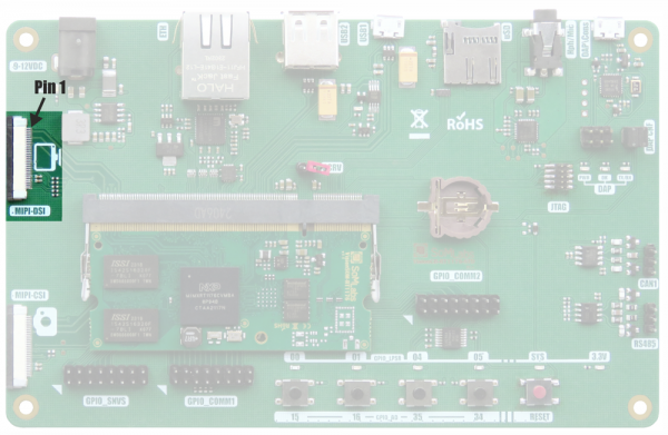
| J501 pin | Default function name | MCU pin name |
|---|---|---|
| 1 | GND | - |
| 2 | DSI.CLK_P | MIPI_DSI_CKP |
| 3 | DSI.CLK_N | MIPI_DSI_CKN |
| 4 | GND | - |
| 5 | DSI.DATA0_P | MIPI_DSI_DP0 |
| 6 | DSI.DATA0_N | MIPI_DSI_DN0 |
| 7 | GND | - |
| 8 | DSI.DATA1_P | MIPI_DSI_DP1 |
| 9 | DSI.DATA1_N | MIPI_DSI_DN1 |
| 10 | GND | - |
| 11 | NC | - |
| 12 | NC | - |
| 13 | GND | - |
| 14 | NC | - |
| 15 | NC | - |
| 16 | GND | |
| 17 | I2C6.SCL1,3 | GPIO_LPSR_07 |
| 18 | I2C6.SDA1,3 | GPIO_LPSR_06 |
| 19 | GND | - |
| 20 | DSI-DISP-RST2 | GPIO5-09 (GPIO_DISP_B2_08) |
| 21 | TP-INT2 | GPIO5-02 (GPIO_DISP_B2_01) |
| 22 | TP-RST2 | GPIO5-01 (GPIO_DISP_B2_00) |
| 23 | GND | - |
| 24 | VDD-3V3 | - |
| 25 | VDD-3V3 | - |
| 26 | VDD-5V0 | - |
| 27 | VDD-5V0 | - |
| 28 | DSI-BL-PWM2 | GPIO3-13 (GPIO_AD_14) |
| 29 | DSI-BL-EN2 | GPIO5-10 (GPIO_DISP_B2_09) |
| 30 | GND | - |
Notes:
1. Both lines pull-upped to 3.3V with 4,7kOhm resistors.
2. In series - between GPIO lines and connector pins - 100 Ohm resistors are included.
3. The I2C6 interface is shared with CSI input.
MIPI-CSI camera connector (J500)
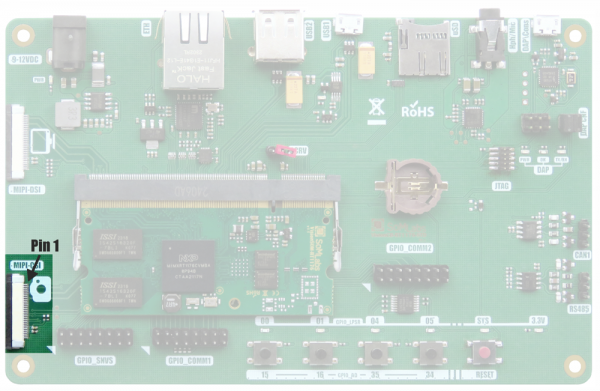
| J500 pin | Default function name | MCU pin name |
|---|---|---|
| 1 | GND | - |
| 2 | CSI.CLK_P | MIPI_CSI_CKP |
| 3 | CSI.CLK_N | MIPI_CSI_CKN |
| 4 | GND | - |
| 5 | CSI.DATA0_P | MIPI_CSI_DP0 |
| 6 | CSI.DATA0_N | MIPI_CSI_DN0 |
| 7 | GND | - |
| 8 | CSI.DATA1_P | MIPI_CSI_DP1 |
| 9 | CSI.DATA1_N | MIPI_CSI_DN1 |
| 10 | GND | - |
| 11 | NC | - |
| 12 | NC | - |
| 13 | GND | - |
| 14 | NC | - |
| 15 | NC | - |
| 16 | GND | |
| 17 | I2C6.SCL1,2 | GPIO_LPSR_07 |
| 18 | I2C6.SDA1,2 | GPIO_LPSR_06 |
| 19 | GND | - |
| 20 | CAM-RES | GPIO5-03 (GPIO_DISP_B2_02) |
| 21 | CAM-PWR-DN | GPIO3-22 (GPIO_AD_23) |
| 22 | - | - |
| 23 | GND | - |
| 24 | VDD-3V3 | - |
| 25 | VDD-3V3 | - |
| 26 | VDD-5V0 | - |
| 27 | VDD-5V0 | - |
| 28 | - | - |
| 29 | - | - |
| 30 | GND | - |
Notes:
1. Both lines pull-upped to 3.3V with 4,7kOhm resistors.
2. The I2C6 interface is shared with DSI output.
RTC/SNVS battery socket (J101)
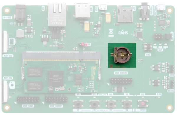
Optional 3V cell (CR2032 or CR2025) for SNVS MCU backup power domain (VDD-COIN-3V).
Dimensions
