StarCB-STM32H757-STD Datasheet and Pinout: Difference between revisions
From SomLabs Wiki
| (125 intermediate revisions by the same user not shown) | |||
| Line 48: | Line 48: | ||
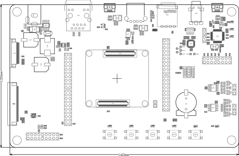
*Board Size: 160mm x 100 mm x 22mm | *Board Size: 160mm x 100 mm x 22mm | ||
== Pictures of StarCB- | == Pictures of StarCB-STM32H757-STD board == | ||
<center> | <center> | ||
{| class="wikitable" | {| class="wikitable" | ||
| Line 54: | Line 54: | ||
! Version !! Photo | ! Version !! Photo | ||
|- | |- | ||
| StarCB- | | StarCB-STM32H757-STD board only || | ||
[[File:StarCB- | [[File:StarCB-STM32H757-no-SoM.png|center|thumb]] | ||
|- | |- | ||
| StarCB- | | StarCB-STM32H757-STD board<br>with StarSOM-STM32H757 installed || | ||
[[File:StarCB- | [[File:StarCB-STM32H757-with-SoM.png|center|thumb]] | ||
|} | |} | ||
</center> | </center> | ||
| Line 72: | Line 67: | ||
{ | { | ||
"type" : "separator", | "type" : "separator", | ||
"value" : "StarCB- | "value" : "StarCB-STM32H757-STD" | ||
} | } | ||
] | ] | ||
| Line 78: | Line 73: | ||
== Block Diagram == | == Block Diagram == | ||
[[File:StarCB- | [[File:StarCB-STM32H757-block.png|1000px|center]] | ||
== Electrical parameters == | == Electrical parameters == | ||
| Line 97: | Line 92: | ||
| 15.0 | | 15.0 | ||
| V | | V | ||
| Positive pole on central connector of | | Positive pole on central connector of J200 | ||
|- | |- | ||
| Supply current | | Supply current | ||
| - | | - | ||
| - | | - | ||
| 0. | | 0.11 | ||
| A | | A | ||
| Excluding SOM, LCD, USB and antoher external loads | | Excluding SOM, LCD, USB and antoher external loads | ||
| Line 114: | Line 109: | ||
</center> | </center> | ||
== Recovery jumper ( | == StarSOM-STM32H757 connectors (J100, J101) == | ||
[[File:StarCB- | [[File:StarCB-STM32H757-SOM.jpg|center|700px]] | ||
== On-board ST-Link debugger (J900) == | |||
[[File:StarCB-STM32H757-USB-STlink.jpg|center|700px]] | |||
== Optional JTAG connector (J903) == | |||
[[File:StarCB-STM32H757-JTAG.jpg|center|700px]] | |||
Notes: | |||
<br>1. JTAG connector pinout is compatible with [https://developer.arm.com/documentation/101416/0100/Hardware-Description/Target-Interfaces/Cortex-Debug--10-pin- Standard Cortex Debug Connector] | |||
<br>2. The recommended 10-pin connector is a Samtec 10-pin FTSH-105-01-L-DV-007-K | |||
<br>3. JTAG connector pins are permanently connected to MCU JTAG lines | |||
== On-board ST-Link debugger connector matrix (J901) == | |||
[[File:StarCB-STM32H757-routing.jpg|center|700px]] | |||
<center> | |||
{| class="wikitable" | |||
! style="text-align: center; font-weight: bold;" | SIDE | |||
! style="text-align: center; font-weight: bold;" | JTAG.TDI | |||
! style="text-align: center; font-weight: bold;" | JTAG.TDO | |||
! style="text-align: center; font-weight: bold;" | JTAG.TCK | |||
! style="text-align: center; font-weight: bold;" | JTAG.TMS | |||
! style="text-align: center; font-weight: bold;" | JTAG.TRST | |||
! style="text-align: center; font-weight: bold;" | RESET | |||
! style="text-align: center; font-weight: bold;" | USART1.RXD | |||
! style="text-align: center; font-weight: bold;" | USART1.TXD | |||
|- | |||
| <b>Top</b> || ST-LINK || ST-LINK || ST-LINK || ST-LINK || ST-LINK || ST-LINK || ST-LINK || ST-LINK | |||
|- | |||
| <b>Bottom</b> || MCU || MCU || MCU || MCU || MCU || MCU || MCU || MCU | |||
|} | |||
</center> | |||
Notes: | |||
<br>1. USART1 - vCOM interface implemented in ST-Link | |||
<br>2. JTAG signals from the MCU side are connected to optional JTAG J903 connector | |||
<br>3. JTAG signals from the MCU side are connected to J101 SoM connector | |||
== Recovery jumper (J803, 2.54mm) == | |||
[[File:StarCB-STM32H757-recovery.jpg|center|700px]] | |||
| Line 131: | Line 164: | ||
Note: | Note: | ||
<br>1. To start recovery procedure connect pins 1 and 2 of | <br>1. To start recovery procedure connect pins 1 and 2 of J803 and press RESET (red) button. | ||
== USB | == Host USB interface (J301) == | ||
[[File:StarCB- | [[File:StarCB-STM32H757-USB-A.jpg|center|700px]] | ||
<br>1. Connector | Notes: | ||
<br>1. Connector J301 (4-pin USB-A) is connected to USB2 MCU transceiver. | |||
<br>2. Power Enable input of USB power switch is connected to PORTB.1. | |||
<br> | <br>3. Overload of power switch is indicated by the LED (D300, USB-OC) lighting. | ||
<br> | |||
== | == USB-OTG interface (J300) == | ||
[[File:StarCB- | [[File:StarCB-STM32H757-USB-OTG.jpg|center|700px]] | ||
Notes: | |||
<br>1. Connector J300 (5-pin MicroUSB) is connected to USB1 MCU transceiver. | |||
<br>2. Power Enable input of USB power switch is connected to PORTB.2. | |||
<br>3. Overload of power switch is indicated by the LED (D300, USB-OC) lighting. | |||
<br>4. Port direction is controlled by USB1.ID line. | |||
== Battery socket (J102, CR1220) == | |||
[[File:StarCB-STM32H757-battery.jpg|center|700px]] | |||
== GPIO #1 connector (J503, 2x20 gold-pin, 2.54mm) == | |||
[[File:StarCB-STM32H757-gpio1.jpg|center|700px]] | |||
<center> | <center> | ||
| Line 152: | Line 195: | ||
! style="text-align: center; font-weight: bold;" | Description | ! style="text-align: center; font-weight: bold;" | Description | ||
|- | |- | ||
| 1 || | | 1 || VDD-3V3 || Power supply for external loads (up to 200 mA<sup>1</sup>) | ||
|- | |||
| 2 || GND || - | |||
|- | |- | ||
| | | 3 || LCD.B0 || LCD controller line, also available on connector J500 (14b RGB LCD Connector) | ||
|- | |- | ||
| | | 4 || LCD.B1 || LCD controller line, also available on connector J500 (14b RGB LCD Connector) | ||
|- | |- | ||
| | | 5 || LCD.B2 || LCD controller line, also available on connector J500 (14b RGB LCD Connector) | ||
|- | |- | ||
| | | 6 || LCD.B3 || LCD controller line, also available on connector J500 (14b RGB LCD Connector) | ||
|- | |- | ||
| | | 7 || LCD.B4 || LCD controller line, also available on connector J500 (14b RGB LCD Connector) | ||
|- | |- | ||
| | | 8 || LCD.B5 || LCD controller line, also available on connector J500 (14b RGB LCD Connector) | ||
|- | |- | ||
| | | 9 || LCD.B6 || LCD controller line, also available on connector J500 (14b RGB LCD Connector) | ||
|- | |- | ||
| | | 10 || LCD.B7 || LCD controller line, also available on connector J500 (14b RGB LCD Connector) | ||
|- | |- | ||
| 10 || | | 11 || LCD.G0 || LCD controller line, also available on connector J500 (14b RGB LCD Connector) | ||
|- | |||
| 12 || LCD.G1 || LCD controller line, also available on connector J500 (14b RGB LCD Connector) | |||
|- | |||
| 13 || LCD.G2 || LCD controller line, also available on connector J500 (14b RGB LCD Connector) | |||
|- | |||
| 14 || LCD.G3 || LCD controller line, also available on connector J500 (14b RGB LCD Connector) | |||
|- | |||
| 15 || LCD.G4 || LCD controller line, also available on connector J500 (14b RGB LCD Connector) | |||
|- | |||
| 16 || LCD.G5 || LCD controller line, also available on connector J500 (14b RGB LCD Connector) | |||
|- | |||
| 17 || LCD.G6 || LCD controller line, also available on connector J500 (14b RGB LCD Connector) | |||
|- | |||
| 18 || LCD.G7 || LCD controller line, also available on connector J500 (14b RGB LCD Connector) | |||
|- | |||
| 19 || LCD.R0 || LCD controller line, also available on connector J500 (14b RGB LCD Connector) | |||
|- | |||
| 20 || LCD.R1 || LCD controller line, also available on connector J500 (14b RGB LCD Connector) | |||
|- | |||
| 21 || LCD.R2 || LCD controller line, also available on connector J500 (14b RGB LCD Connector) | |||
|- | |||
| 22 || LCD.R3 || LCD controller line, also available on connector J500 (14b RGB LCD Connector) | |||
|- | |||
| 23 || LCD.R4 || LCD controller line, also available on connector J500 (14b RGB LCD Connector) | |||
|- | |||
| 24 || LCD.R5 || LCD controller line, also available on connector J500 (14b RGB LCD Connector) | |||
|- | |||
| 25 || LCD.R6 || LCD controller line, also available on connector J500 (14b RGB LCD Connector) | |||
|- | |||
| 26 || LCD.R7 || LCD controller line, also available on connector J500 (14b RGB LCD Connector) | |||
|- | |||
| 27 || LCD.DE || LCD controller line, also available on connector J500 (14b RGB LCD Connector) | |||
|- | |||
| 28 || LCD.HSYNC || LCD controller line, also available on connector J500 (14b RGB LCD Connector) | |||
|- | |||
| 29 || LCD.VSYNC || LCD controller line, also available on connector J500 (14b RGB LCD Connector) | |||
|- | |||
| 30 || LCD.CLK || LCD controller line, also available on connector J500 (14b RGB LCD Connector) | |||
|- | |||
| 31 || - || - | |||
|- | |||
| 32 || - || - | |||
|- | |||
| 33 || PORTB.10 || Touch-panel interrupt line, also available on connectors J500 (14b RGB LCD Connector) and J501 (MIPI-DSI) | |||
|- | |||
| 34 || PORTH.11 || LCD backlight PWM controller line, also available on connectors J500 (14b RGB LCD Connector) and J501 (MIPI-DSI) | |||
|- | |||
| 35 || PORTB.11 || LCD backlight on/off controller line, also available on connectors J500 (14b RGB LCD Connector) and J501 (MIPI-DSI) | |||
|- | |||
| 36 || PORTH.6 || Touch-panel reset line, also available on connectors J500 (14b RGB LCD Connector) and J501 (MIPI-DSI) | |||
|- | |||
| 37 || - || - | |||
|- | |||
| 38 || PORTB.0 || LCD reset line, also available on connectors J500 (14b RGB LCD Connector) and J501 (MIPI-DSI) | |||
|- | |||
| 39 || I2C3.SCL || Touch-panel I2C interface, also available on connectors J500 (14b RGB LCD Connector) and J501 (MIPI-DSI)<br>With 2.2kOhm pull-up | |||
|- | |||
| 40 || I2C3.SDA || Touch-panel I2C interface, also available on connectors J500 (14b RGB LCD Connector) and J501 (MIPI-DSI)<br>With 2.2kOhm pull-up | |||
|} | |} | ||
</center> | </center> | ||
<br>Note: | |||
<br>1. 200 mA is the total load value for 3.3V line | |||
== GPIO connector ( | == GPIO #2 connector (J801, 2x20 gold-pin, 2.54mm) == | ||
[[File:StarCB- | [[File:StarCB-STM32H757-gpio2.jpg|center|700px]] | ||
<center> | <center> | ||
| Line 183: | Line 288: | ||
! style="text-align: center; font-weight: bold;" | Description | ! style="text-align: center; font-weight: bold;" | Description | ||
|- | |- | ||
| 1 || VDD-3V3 || Power supply for external loads (up to | | 1 || VDD-3V3 || Power supply for external loads (up to 200 mA<sup>1</sup>) | ||
|- | |- | ||
| 2 || | | 2 || GND || - | ||
|- | |- | ||
| 3 || | | 3 || UART2X.TXD || - | ||
|- | |- | ||
| 4 || | | 4 || UART2X.RXD || - | ||
|- | |- | ||
| 5 || | | 5 || UART2X.RTS || - | ||
|- | |- | ||
| 6 || | | 6 || UART2X.RTS || - | ||
|- | |- | ||
| 7 || | | 7 || PORTC.7 || - | ||
|- | |- | ||
| 8 || | | 8 || PORTI.14 || Line connected to user Card Detect signal of J800 | ||
|- | |- | ||
| 9 || | | 9 || PORTI.8 || - | ||
|- | |- | ||
| 10 || | | 10 || PORTI.9 || - | ||
|- | |- | ||
| 11 || | | 11 || PORTI.10|| - | ||
|- | |- | ||
| 12 || | | 12 || - || - | ||
|- | |- | ||
| 13 || | | 13 || - || - | ||
|- | |- | ||
| 14 || | | 14 || - || - | ||
|- | |- | ||
| 15 || | | 15 || CAN1.TX || Tx line of CAN interface (MCP2542FD)<br>Connected to CAN-FD PHY interface | ||
|- | |- | ||
| 16 || | | 16 || CAN1.RX || Rx line of CAM interface ((MCP2542FD)<br>Connected to CAN-FD PHY interface | ||
|- | |- | ||
| 17 || | | 17 || PORTG.9 || RxD of RS-485 interface (USART6.RX)<br>Connected to RS-485 PHY interface | ||
|- | |- | ||
| 18 || | | 18 || PORTG.14 || TxD of RS-485 interface (USART6.TX)<br>Connected to RS-485 PHY interface | ||
|- | |- | ||
| 19 || | | 19 || PORTD.7 || Data Enable (transmit enable) line of RS-485 interface<br>Connected to RS-485 PHY interface | ||
|- | |- | ||
| 20 || | | 20 || PORTB.5 || Optional Standby signal of CAN interface (MCP2542FD)<br>Connected to CAN-FD PHY interface | ||
|- | |- | ||
| 21 || | | 21 || PORTE.3 || Camera reset signal | ||
|- | |- | ||
| 22 || | | 22 || PORTE.5 || Line connected to user LED D804 | ||
|- | |- | ||
| 23 || | | 23 || I2C1.SDA || Audio codec control interface<br>Pulled-upwith 2.2kOhm | ||
|- | |- | ||
| 24 || | | 24 || I2C1.SCL || Audio codec control interface<br>Pulled-upwith 2.2kOhm | ||
|- | |- | ||
| 25 || | | 25 || PORTE.6 || Line connected to user LED D803 | ||
|- | |- | ||
| 26 || | | 26 || PORTI.11 || Line connected to user LED D802 | ||
|- | |- | ||
| 27 || | | 27 || PORTH.2 || Line connected to switch S803 | ||
|- | |- | ||
| 28 || | | 28 || PORTH.3 || Line connected to switch S802 | ||
|- | |- | ||
| 29 || | | 29 || PORTH.4 || Line connected to switch S801 | ||
|- | |- | ||
| 30 || | | 30 || PORTH.5 || Line connected to switch S800 | ||
|- | |- | ||
| 31 || | | 31 || PORTA.5 || Line connected to user LED D801 | ||
|- | |- | ||
| 32 || | | 32 || PORTA.0 || Line connected to user LED D800 | ||
|- | |- | ||
| 33 || | | 33 || PC2_C || - | ||
|- | |- | ||
| 34 || | | 34 || PC3_C || - | ||
|- | |- | ||
| 35 || | | 35 || PA0_C || - | ||
|- | |- | ||
| 36 || | | 36 || PA1_C || - | ||
|- | |- | ||
| 37 || | | 37 || UART7.CTS || - | ||
|- | |- | ||
| 38 || | | 38 || UART7.RTS || - | ||
|- | |- | ||
| 39 || | | 39 || UART7.RXD || - | ||
|- | |- | ||
| 40 || | | 40 || UART7.TXD || - | ||
|} | |} | ||
</center> | </center> | ||
<br>Note: | |||
<br>1. 200 mA is the total load value for 3.3V line | |||
== | == RGB display interface (J500, FPC/FFC 0.5mm) == | ||
[[File:StarCB- | [[File:StarCB-STM32H757-RGB.jpg|center|700px]] | ||
<center> | <center> | ||
| Line 274: | Line 381: | ||
! style="text-align: center; font-weight: bold;" | Description | ! style="text-align: center; font-weight: bold;" | Description | ||
|- | |- | ||
| 1 || LCD. | | 1 || LCD.B0 || - | ||
|- | |- | ||
| 2 || LCD. | | 2 || LCD.B1 || - | ||
|- | |- | ||
| 3 || LCD. | | 3 || LCD.B2 || - | ||
|- | |- | ||
| 4 || LCD. | | 4 || LCD.B3 || - | ||
|- | |- | ||
| 5 || LCD. | | 5 || LCD.B4 || - | ||
|- | |- | ||
| 6 || LCD. | | 6 || LCD.B5 || - | ||
|- | |- | ||
| 7 || LCD. | | 7 || LCD.B6 || - | ||
|- | |- | ||
| 8 || LCD. | | 8 || LCD.B7 || - | ||
|- | |- | ||
| 9 || GND || - | | 9 || GND || - | ||
|- | |- | ||
| 10 || LCD. | | 10 || LCD.G0 || - | ||
|- | |- | ||
| 11 || LCD. | | 11 || LCD.G1 || - | ||
|- | |- | ||
| 12 || LCD. | | 12 || LCD.G2 || - | ||
|- | |- | ||
| 13 || LCD. | | 13 || LCD.G3 || - | ||
|- | |- | ||
| 14 || LCD. | | 14 || LCD.G4 || - | ||
|- | |- | ||
| 15 || LCD. | | 15 || LCD.G5 || - | ||
|- | |- | ||
| 16 || LCD. | | 16 || LCD.G6 || - | ||
|- | |- | ||
| 17 || LCD. | | 17 || LCD.G7 || - | ||
|- | |- | ||
| 18 || GND || - | | 18 || GND || - | ||
|- | |- | ||
| 19 || LCD. | | 19 || LCD.R0 || - | ||
|- | |- | ||
| 20 || LCD. | | 20 || LCD.R1 || - | ||
|- | |- | ||
| 21 || LCD. | | 21 || LCD.R2 || - | ||
|- | |- | ||
| 22 || LCD. | | 22 || LCD.R3 || - | ||
|- | |- | ||
| 23 || LCD. | | 23 || LCD.R4 || - | ||
|- | |- | ||
| 24 || LCD. | | 24 || LCD.R5 || - | ||
|- | |- | ||
| 25 || LCD. | | 25 || LCD.R6 || - | ||
|- | |- | ||
| 26 || LCD. | | 26 || LCD.R7 || - | ||
|- | |- | ||
| 27 || GND || - | | 27 || GND || - | ||
|- | |- | ||
| 28 || LCD. | | 28 || LCD.DE || - | ||
|- | |- | ||
| 29 || LCD.HSYNC || - | | 29 || LCD.HSYNC || - | ||
| Line 340: | Line 447: | ||
| 33 || GND || - | | 33 || GND || - | ||
|- | |- | ||
| 34 || | | 34 || - || - | ||
|- | |- | ||
| 35 || | | 35 || - || - | ||
|- | |- | ||
| 36 || | | 36 || PORTB.10 || Touch-panel interrupt line, also available on connector J501 (MIPI-DSI) | ||
|- | |- | ||
| 37 || | | 37 || PORTH.11 || LCD backlight PWM controller line, also available on connector J501 (MIPI-DSI) | ||
|- | |- | ||
| 38 || - || - | | 38 || - || - | ||
| Line 356: | Line 463: | ||
| 41 || - || - | | 41 || - || - | ||
|- | |- | ||
| 42 || | | 42 || I2C3.SCL || Touch-panel I2C interface, also available on connector J501 (MIPI-DSI) and J502 (Camera) and J503 (GPIO #1)<br>With 2.2kOhm pull-up | ||
|- | |- | ||
| 43 || | | 43 || I2C3.SDA || Touch-panel I2C interface, also available on connector J501 (MIPI-DSI) and J502 (Camera) and J503 (GPIO #1)<br>With 2.2kOhm pull-up | ||
|- | |- | ||
| 44 || GND || - | | 44 || GND || - | ||
|- | |- | ||
| 45 || VDD- | | 45 || VDD-5V0 || +5.0V power source for LCD module | ||
|- | |||
| 46 || VDD-5V0 || +5.0V power source for LCD module | |||
|- | |||
| 47 || VDD-5V0 || +5.0V power source for LCD module | |||
|- | |||
| 48 || VDD-5V0 || +5.0V power source for LCD module | |||
|- | |||
| 49 || PORTH.6 || Touch-panel reset line, also available on connector J501 (MIPI-DSI) | |||
|- | |||
| 50 || PORTB.11 || LCD backlight on/off controller line, also available on connector J501 (MIPI-DSI) | |||
|} | |||
</center> | |||
== MIPI-DSI display interface (J501, FPC/FFC 0.5mm) == | |||
[[File:StarCB-STM32H757-MIPI-DSI.jpg|center|700px]] | |||
<center> | |||
{| class="wikitable" | |||
! style="text-align: center; font-weight: bold;" | Pin | |||
! style="text-align: center; font-weight: bold;" | Signal | |||
! style="text-align: center; font-weight: bold;" | Description | |||
|- | |||
| 1 || GND || - | |||
|- | |||
| 2 || DSI.CK_P || - | |||
|- | |||
| 3 || DSI.CK_N || - | |||
|- | |||
| 4 || GND || - | |||
|- | |||
| 5 || DSI.D0_P || - | |||
|- | |||
| 6 || DSI.D0_N || - | |||
|- | |||
| 7 || GND || - | |||
|- | |||
| 8 || DSI.D1_P || - | |||
|- | |||
| 9 || DSI.D1_N || - | |||
|- | |||
| 10 || GND || - | |||
|- | |||
| 11 || - || - | |||
|- | |||
| 12 || - || - | |||
|- | |||
| 13 || GND || - | |||
|- | |||
| 14 || - || - | |||
|- | |||
| 15 || - || - | |||
|- | |||
| 16 || GND || - | |||
|- | |||
| 17 || I2C3.SCL || Touch-panel I2C interface, also available on connector J500 (14b RGB LCD Connector) and J502 (Camera) and J503 (GPIO #1)<br>With 2.2kOhm pull-up | |||
|- | |||
| 18 || I2C3.SDA || Touch-panel I2C interface, also available on connector J500 (14b RGB LCD Connector) and J502 (Camera) and J503 (GPIO #1)<br>With 2.2kOhm pull-up | |||
|- | |||
| 19 || GND || - | |||
|- | |||
| 20 || PORTB.0 || LCD reset line, also available on connector J500 (14b RGB LCD Connector) | |||
|- | |||
| 21 || PORTB.10 || Touch-panel interrupt line, also available on connectors J500 (14b RGB LCD Connector) | |||
|- | |||
| 22 || PORTH.6 || Touch-panel reset line, also available on connector connector J500 (14b RGB LCD Connector) | |||
|- | |||
| 23 || GND || - | |||
|- | |||
| 24 || VDD-5V0 || +5.0V power source for LCD module | |||
|- | |||
| 25 || VDD-5V0 || +5.0V power source for LCD module | |||
|- | |||
| 26 || VDD-5V0 || +5.0V power source for LCD module | |||
|- | |||
| 27 || VDD-5V0 || +5.0V power source for LCD module | |||
|- | |||
| 28 || PORTH.11 || LCD backlight PWM controller line, also available on connector J500 (14b RGB LCD Connector) | |||
|- | |||
| 29 || PORTB.11 || LCD backlight on/off controller line, also available on connector connector J500 (14b RGB LCD Connector) | |||
|- | |||
| 30 || GND || - | |||
|- | |||
|} | |||
</center> | |||
== Parallel camera interface (J502, 2x9 gold-pin, 2.54mm) == | |||
[[File:StarCB-STM32H757-CAMERA.jpg|center|700px]] | |||
<center> | |||
{| class="wikitable" | |||
! style="text-align: center; font-weight: bold;" | Pin | |||
! style="text-align: center; font-weight: bold;" | Signal | |||
! style="text-align: center; font-weight: bold;" | Description | |||
|- | |||
| 1 || VDD-3V3|| Power supply for external loads (up to 200 mA<sup>1</sup>) | |||
|- | |||
| 2 || GND || - | |||
|- | |||
| 3 || I2C3.SCL || Touch-panel I2C interface, also available on connectors J500 (14b RGB LCD Connector) and J501 (MIPI-DSI) and J503 (GPIO #1)<br>With 2.2kOhm pull-up | |||
|- | |||
| 4 || I2C3.SDA || Touch-panel I2C interface, also available on connectors J500 (14b RGB LCD Connector) and J501 (MIPI-DSI) and J503<br>With 2.2kOhm pull-up | |||
|- | |||
| 5 || DCAM.VSYNC || - | |||
|- | |||
| 6 || DCAM.HSYNC || - | |||
|- | |||
| 7 || DCAM.PCLK || - | |||
|- | |||
| 8 || CAM-XCLK || On-board 24 MHz clock generator | |||
|- | |||
| 9 || DCAM.D7 || - | |||
|- | |||
| 10 || DCAM.D6 || - | |||
|- | |||
| 11 || DCAM.D5 || - | |||
|- | |- | ||
| | | 12 || DCAM.D4 || - | ||
|- | |- | ||
| | | 13 || DCAM.D3 || - | ||
|- | |- | ||
| | | 14 || DCAM.D2 || - | ||
|- | |- | ||
| | | 15 || DCAM.D1 || - | ||
|- | |||
| 16 || DCAM.D0 || - | |||
|- | |||
| 17 || CAM-RST || PORTE.3 - camera reset line | |||
|- | |||
| 18 || CAM-PWD || 3.3V power supply for camera module | |||
|- | |- | ||
|} | |} | ||
</center> | </center> | ||
<br>Note: | |||
<br>1. 200 mA is the total load value for 3.3V line | |||
<br>2. Example recommended camera module is [https://kamami.pl/en/cameras/1188465-ov5640-camera-breakout-ov5640-camera-module-with-120-lens-and-autofocus-5906623490622.html OV5640 Camera Breakout] | |||
== | |||
[[File:StarCB- | == CAN-FD interface (J700, 1x3 gold-pin, 2.54mm) == | ||
[[File:StarCB-STM32H757-CAN.jpg|center|700px]] | |||
<br> | |||
<center> | <center> | ||
J700 connector pinout | |||
{| class="wikitable" | {| class="wikitable" | ||
! style="text-align: center; font-weight: bold;" | | ! style="text-align: center; font-weight: bold;" | Pin | ||
! style="text-align: center; font-weight: bold;" | | ! style="text-align: center; font-weight: bold;" | Signal | ||
! style="text-align: center; font-weight: bold;" | Description | ! style="text-align: center; font-weight: bold;" | Description | ||
|- | |- | ||
| | | 1 || GND || - | ||
|- | |||
| 2 || L || CAN L signal Line | |||
|- | |||
| 3 || H || CAN H signal Line | |||
|- | |||
|} | |||
</center> | |||
<center> | |||
CAN-FD interface connections to MCU | |||
{| class="wikitable" | |||
! style="text-align: center; font-weight: bold;" | Pin | |||
! style="text-align: center; font-weight: bold;" | Signal | |||
! style="text-align: center; font-weight: bold;" | Description | |||
! style="text-align: center; font-weight: bold;" | Note | |||
|- | |||
| 63 (J101) || CAN1.TX || CAN-FD Transmit Data || Connected to GPIO #2 connector | |||
|- | |||
| 61 (J101) || CAN1.TX || CAN-FD Receive Data || Connected to GPIO #2 connector | |||
|- | |||
| 53 (J101)|| PORTB.5 || CAN-FD PHY layer STB signal || Connected to GPIO #2 connector | |||
|- | |||
|} | |||
</center> | |||
== RS-485 interface (J701, 1x3 gold-pin, 2.54mm) == | |||
[[File:StarCB-STM32H757-RS485.jpg|center|700px]] | |||
<br> | |||
<center> | |||
J700 connector pinout | |||
{| class="wikitable" | |||
! style="text-align: center; font-weight: bold;" | Pin | |||
! style="text-align: center; font-weight: bold;" | Signal | |||
! style="text-align: center; font-weight: bold;" | Description | |||
|- | |||
| 1 || GND || - | |||
|- | |||
| 2 || L || CAN L signal Line | |||
|- | |||
| 3 || H || CAN H signal Line | |||
|- | |||
|} | |||
</center> | |||
<br> | |||
<center> | |||
CAN-FD interface connections to MCU | |||
{| class="wikitable" | |||
! style="text-align: center; font-weight: bold;" | Pin | |||
! style="text-align: center; font-weight: bold;" | Signal | |||
! style="text-align: center; font-weight: bold;" | Description | |||
! style="text-align: center; font-weight: bold;" | Note | |||
|- | |||
| 63 (J101) || CAN1.TX || CAN-FD Transmit Data || Connected to GPIO #2 connector | |||
|- | |||
| 61 (J101) || CAN1.TX || CAN-FD Receive Data || Connected to GPIO #2 connector | |||
|- | |||
| 53 (J101)|| PORTB.5 || CAN-FD PHY layer STB signal || Connected to GPIO #2 connector | |||
|- | |- | ||
|} | |} | ||
</center> | </center> | ||
== Audio codec (J600, MiniJack) == | |||
< | [[File:StarCB-STM32H757-codec.jpg|center|700px]] | ||
< | |||
<center> | |||
{| class="wikitable" | |||
! style="text-align: center; font-weight: bold;" | Pin | |||
! style="text-align: center; font-weight: bold;" | Signal | |||
! style="text-align: center; font-weight: bold;" | Description | |||
! style="text-align: center; font-weight: bold;" | Note | |||
|- | |||
| 98 (J101) || I2S2.MCK || NAU88C22YG codec signal || - | |||
|- | |||
| 90 (J101) || I2S2.CK || NAU88C22YG codec signal || - | |||
|- | |||
| 88 (J101)|| I2S2.WS || NAU88C22YG codec signal || - | |||
|- | |||
| 94 (J101)|| I2S2.SDO || NAU88C22YG codec signal || - | |||
|- | |||
| 92 (J101)|| I2S2.SDI || NAU88C22YG codec signal || - | |||
|- | |||
| 35 (J101)|| I2C1.SCL || NAU88C22YG control interface || Connected to GPIO #2 connector | |||
|- | |||
| 37 (J101)|| I2C1.SDA || NAU88C22YG control interface || Connected to GPIO #2 connector | |||
|- | |||
|} | |||
</center> | |||
== Ethernet interface (J302, RJ-45) == | |||
[[File:StarCB-STM32H757-ETH.jpg|center|700px]] | |||
<center> | <center> | ||
{| class="wikitable" | {| class="wikitable" | ||
! style="text-align: center; font-weight: bold;" | | ! style="text-align: center; font-weight: bold;" | Pin | ||
! style="text-align: center; font-weight: bold;" | | ! style="text-align: center; font-weight: bold;" | Signal | ||
! style="text-align: center; font-weight: bold;" | Description | ! style="text-align: center; font-weight: bold;" | Description | ||
! style="text-align: center; font-weight: bold;" | Note | |||
|- | |- | ||
| | | 65 (J100) || ETH.TX_p || J302 TD+ pin 1 || 10/100 Mb Ethernet connector | ||
|- | |- | ||
| | | 67 (J100) || ETH.TX_n || J302 TD- pin 2 || 10/100 Mb Ethernet connector | ||
|- | |- | ||
| | | 71 (J100) || ETH.RX_p || J302 RD+ pin 3 || 10/100 Mb Ethernet connector | ||
|- | |||
| 73 (J100) || ETH.RX_n || J302 RD- pin 6 || 10/100 Mb Ethernet connector | |||
|- | |||
| 59 (J100) || ETH.LED0 || Green LED || - | |||
|- | |||
| 61 (J100) || ETH.LED1 || Yellow LED || - | |||
|- | |- | ||
|} | |} | ||
</center> | |||
== SD card interface (J800) == | |||
[[File:StarCB-STM32H757-uSD.jpg|center|700px]] | |||
<center> | |||
{| class="wikitable" | {| class="wikitable" | ||
! style="text-align: center; font-weight: bold;" | | ! style="text-align: center; font-weight: bold;" | Pin | ||
! style="text-align: center; font-weight: bold;" | Signal | ! style="text-align: center; font-weight: bold;" | Signal | ||
! style="text-align: center; font-weight: bold;" | Description | ! style="text-align: center; font-weight: bold;" | Description | ||
! style="text-align: center; font-weight: bold;" | Note | |||
|- | |||
| 89 (J101) || SDMMC.D0 || - || - | |||
|- | |||
| 87 (J101) || SDMMC.D1 || - || - | |||
|- | |||
| 97 (J101) || SDMMC.D2 || - || - | |||
|- | |||
| 95 (J101) || SDMMC.D3 || - || - | |||
|- | |||
| 91 (J101) || SDMMC.CK || - || - | |||
|- | |||
| 93 (J101) || SDMMC.CMD || - || - | |||
|- | |||
| 93 (J101) || SDMMC.CD || Card detect signal || Connected to PORTI.14 GPIO line<br>Available on GPIO #2 connector | |||
|- | |- | ||
|} | |} | ||
</center> | |||
== User switches == | |||
[[File:StarCB-STM32H757-switches.jpg|center|700px]] | |||
<center> | |||
{| class="wikitable" | {| class="wikitable" | ||
! style="text-align: center; font-weight: bold;" | | ! style="text-align: center; font-weight: bold;" | Pin | ||
! style="text-align: center; font-weight: bold;" | | ! style="text-align: center; font-weight: bold;" | Signal | ||
! style="text-align: center; font-weight: bold;" | Description | ! style="text-align: center; font-weight: bold;" | Description | ||
! style="text-align: center; font-weight: bold;" | Note | |||
|- | |||
| 17 (J101) || H.5 || Connected to PORTH.5 || User switch | |||
|- | |||
| 19 (J101) || H.4 || Connected to PORTH.4 || User switch | |||
|- | |- | ||
| | | 21 (J101) || H.3 || Connected to PORTH.3 || User switch | ||
|- | |- | ||
| | | 23 (J101) || H.2 || Connected to PORTH.2 || User switch | ||
|- | |- | ||
| | | 8 (J101) || RESET || Manual reset switch || Connected to JTAG connector and ST-Link debugger MCU reset line | ||
|- | |- | ||
|} | |} | ||
</center> | |||
== User LEDs == | |||
[[File:StarCB-STM32H757-led.jpg|center|700px]] | |||
<center> | |||
{| class="wikitable" | {| class="wikitable" | ||
! style="text-align: center; font-weight: bold;" | | ! style="text-align: center; font-weight: bold;" | Pin | ||
! style="text-align: center; font-weight: bold;" | | ! style="text-align: center; font-weight: bold;" | Signal | ||
! style="text-align: center; font-weight: bold;" | Description | ! style="text-align: center; font-weight: bold;" | Description | ||
! style="text-align: center; font-weight: bold;" | Note | |||
|- | |||
| 17 (J101) || A.0 || Connected to PORTA.0 || User LED, actve "0" | |||
|- | |||
| 19 (J101) || A.5 || Connected to PORTA.5 || User LED, actve "0" | |||
|- | |||
| 21 (J101) || I.11 || Connected to PORTI.11 || User LED, actve "0" | |||
|- | |||
| 23 (J101) || E.6 || Connected to PORTE.6 || User LED, actve "0" | |||
|- | |||
| 39 (J101) || E.5 || Connected to PORTE.5 || User LED, actve "0" | |||
|- | |||
| - || PWR || 3.3V power signalling || Permanantly connected to 3.3V | |||
|- | |- | ||
|} | |} | ||
</center> | </center> | ||
== Power supply connector (J200, 9-12 VDC) == | |||
[[File:StarCB-STM32H757-PWR.jpg|800px|center]] | |||
Note: | |||
<br>1. External power connector type DC-140-B05-00-PN (5.5/2.5 mm) | |||
== Dimensions == | == Dimensions == | ||
[[File:StarCB- | [[File:StarCB-STM32H757-PCB.png|800px|center]] | ||
Latest revision as of 16:13, 7 April 2026

StarCB-STM32H757-STD Datasheet and Pinout
General description
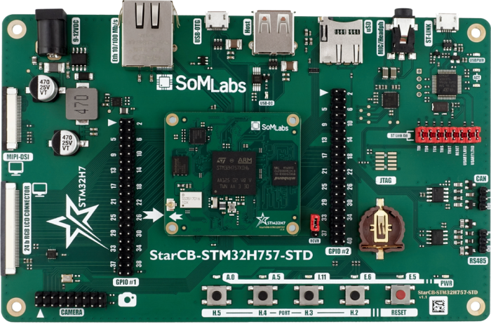
StarCB-STM32H757-STD is a carrier board for the StarSOM-STM32H757 family of computer-on-modules, which are powered by one of the fastest MCU based on Cortex-M cores - STM32H757. A carrier board, together with a System on Module (SoM), makes a complete development platform similar to SBC. The carrier board houses the most common interfaces such as audio codec, USB, Ethernet, UART, RS485, CAN, ST-Link debugger, etc. A large variety of interfaces allows to use it as both a complete development platform or as a stand-alone end-product.
The carrier board connects with the SoM via a board-to-board, low profile connectors.
Applications
- IoT Sensor Hubs
- Home Appliances
- IoT gateways
- Protocol converters
- Home Automation – Smart Home
- Point-of-sales (POS) terminals
- Cash Register
- 2D barcode scanners and printers
- Smart grid infrastructure
- Residential gateways
- Outdoor equipment
Features
- Carrier Board (Base Board) compatible with the StarSOM-STM32H757 family of modules based on STM32H757XI MCU
- SoM Interface: 2x100 board-to-board connectors
- Debug Interface: ST-Link (vCOM/USB)
- Expansion Connectors:
- QSPI connector 2x10 Pin Header (Male)
- GPIO connector 2x20 Pin Header (Male)
- Communication Connectors:
- 1x Ethernet 10/100 Mbit/s, RJ45
- 1x USB Host Type A connectors
- 1x USB OTG Micro AB connector
- 1x Console MicroUSB B connector
- 1x half-duplex RS485
- 1x CAN-FD
- Display and Multimedia Interface:
- 50-pin FFC/FPC parallel RGB (up to 24 bits)
- 30-pin FFC/FPC MIPI-DSI
- codec audio
- parallel 8-bit CCD camera
- User Interface:
- 4+1 Pushbuttons
- 4+1 LEDs
- Expansion Connectors:
- GPIO 2x40
- External Power Supply 9-12V DC
- Temperature Range: 0 to +70°C
- Board Size: 160mm x 100 mm x 22mm
Pictures of StarCB-STM32H757-STD board
| Version | Photo |
|---|---|
| StarCB-STM32H757-STD board only |
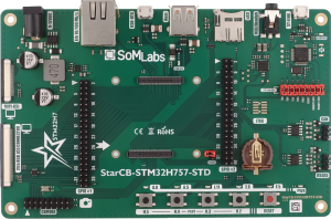 |
| StarCB-STM32H757-STD board with StarSOM-STM32H757 installed |
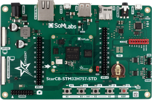 |
Ordering info
Block Diagram
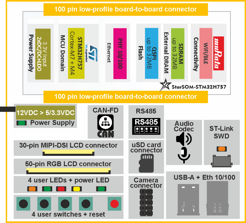
Electrical parameters
| Parameter | Value | Units | Comment | ||
|---|---|---|---|---|---|
| Min. | Typ. | Max. | |||
| Power Supply | 9.0 | 12.0 | 15.0 | V | Positive pole on central connector of J200 |
| Supply current | - | - | 0.11 | A | Excluding SOM, LCD, USB and antoher external loads |
| GPIO voltage | 3.3 | V | |||
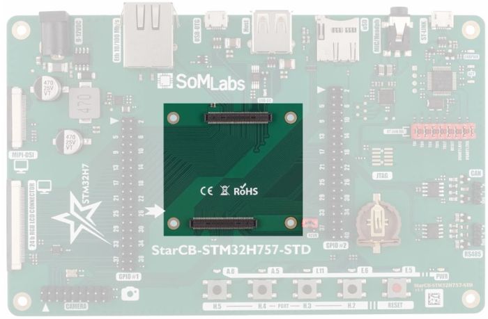
StarSOM-STM32H757 connectors (J100, J101)
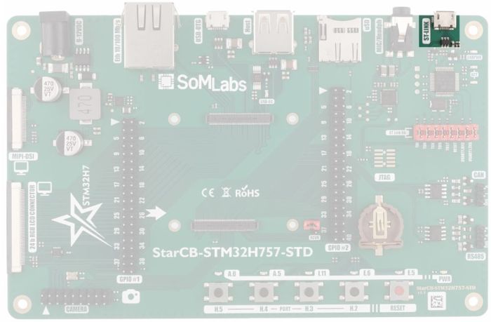
On-board ST-Link debugger (J900)
Optional JTAG connector (J903)
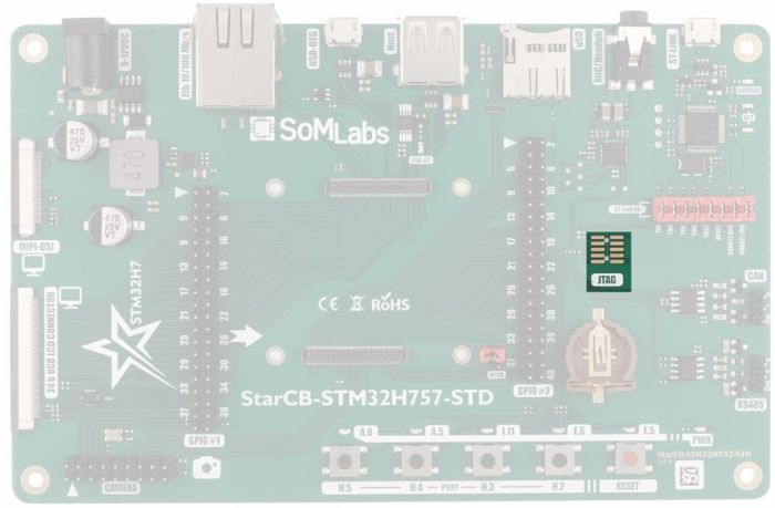
Notes:
1. JTAG connector pinout is compatible with Standard Cortex Debug Connector
2. The recommended 10-pin connector is a Samtec 10-pin FTSH-105-01-L-DV-007-K
3. JTAG connector pins are permanently connected to MCU JTAG lines
On-board ST-Link debugger connector matrix (J901)
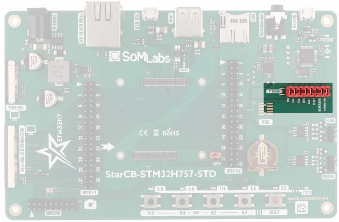
| SIDE | JTAG.TDI | JTAG.TDO | JTAG.TCK | JTAG.TMS | JTAG.TRST | RESET | USART1.RXD | USART1.TXD |
|---|---|---|---|---|---|---|---|---|
| Top | ST-LINK | ST-LINK | ST-LINK | ST-LINK | ST-LINK | ST-LINK | ST-LINK | ST-LINK |
| Bottom | MCU | MCU | MCU | MCU | MCU | MCU | MCU | MCU |
Notes:
1. USART1 - vCOM interface implemented in ST-Link
2. JTAG signals from the MCU side are connected to optional JTAG J903 connector
3. JTAG signals from the MCU side are connected to J101 SoM connector
Recovery jumper (J803, 2.54mm)
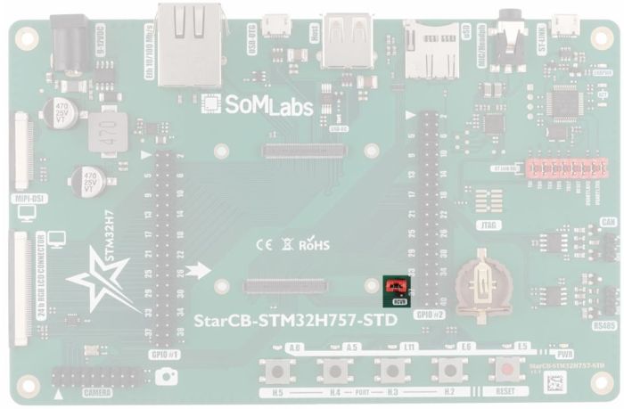
| Pin | Signal | Description |
|---|---|---|
| 1 | Recovery | SOM recovery input |
| 2 | GND |
Note:
1. To start recovery procedure connect pins 1 and 2 of J803 and press RESET (red) button.
Host USB interface (J301)
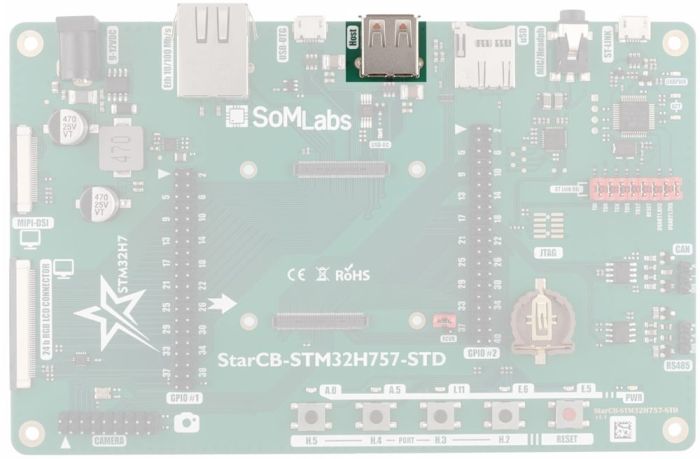
Notes:
1. Connector J301 (4-pin USB-A) is connected to USB2 MCU transceiver.
2. Power Enable input of USB power switch is connected to PORTB.1.
3. Overload of power switch is indicated by the LED (D300, USB-OC) lighting.
USB-OTG interface (J300)
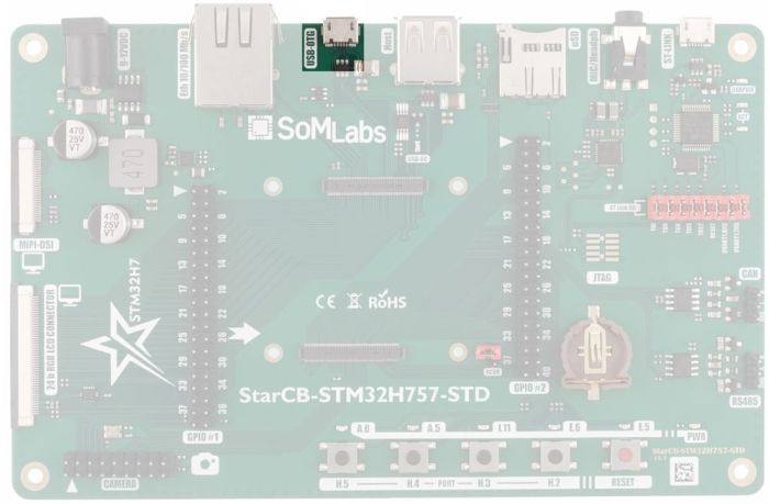
Notes:
1. Connector J300 (5-pin MicroUSB) is connected to USB1 MCU transceiver.
2. Power Enable input of USB power switch is connected to PORTB.2.
3. Overload of power switch is indicated by the LED (D300, USB-OC) lighting.
4. Port direction is controlled by USB1.ID line.
Battery socket (J102, CR1220)
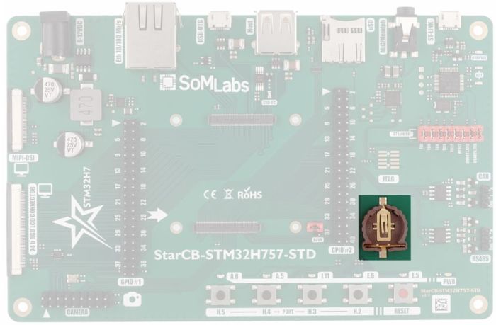
GPIO #1 connector (J503, 2x20 gold-pin, 2.54mm)
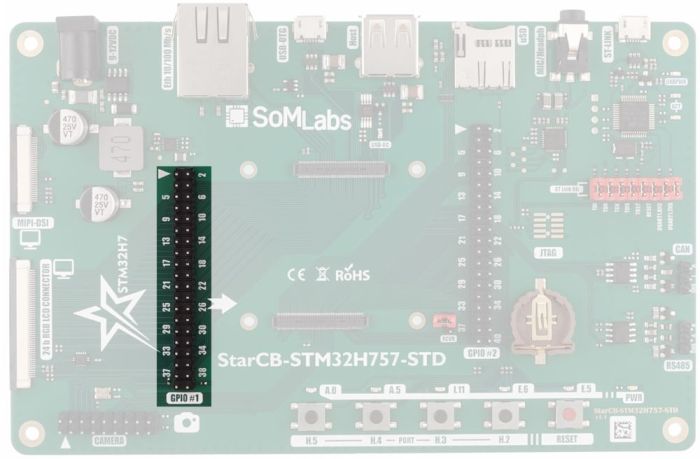
| Pin | Signal | Description |
|---|---|---|
| 1 | VDD-3V3 | Power supply for external loads (up to 200 mA1) |
| 2 | GND | - |
| 3 | LCD.B0 | LCD controller line, also available on connector J500 (14b RGB LCD Connector) |
| 4 | LCD.B1 | LCD controller line, also available on connector J500 (14b RGB LCD Connector) |
| 5 | LCD.B2 | LCD controller line, also available on connector J500 (14b RGB LCD Connector) |
| 6 | LCD.B3 | LCD controller line, also available on connector J500 (14b RGB LCD Connector) |
| 7 | LCD.B4 | LCD controller line, also available on connector J500 (14b RGB LCD Connector) |
| 8 | LCD.B5 | LCD controller line, also available on connector J500 (14b RGB LCD Connector) |
| 9 | LCD.B6 | LCD controller line, also available on connector J500 (14b RGB LCD Connector) |
| 10 | LCD.B7 | LCD controller line, also available on connector J500 (14b RGB LCD Connector) |
| 11 | LCD.G0 | LCD controller line, also available on connector J500 (14b RGB LCD Connector) |
| 12 | LCD.G1 | LCD controller line, also available on connector J500 (14b RGB LCD Connector) |
| 13 | LCD.G2 | LCD controller line, also available on connector J500 (14b RGB LCD Connector) |
| 14 | LCD.G3 | LCD controller line, also available on connector J500 (14b RGB LCD Connector) |
| 15 | LCD.G4 | LCD controller line, also available on connector J500 (14b RGB LCD Connector) |
| 16 | LCD.G5 | LCD controller line, also available on connector J500 (14b RGB LCD Connector) |
| 17 | LCD.G6 | LCD controller line, also available on connector J500 (14b RGB LCD Connector) |
| 18 | LCD.G7 | LCD controller line, also available on connector J500 (14b RGB LCD Connector) |
| 19 | LCD.R0 | LCD controller line, also available on connector J500 (14b RGB LCD Connector) |
| 20 | LCD.R1 | LCD controller line, also available on connector J500 (14b RGB LCD Connector) |
| 21 | LCD.R2 | LCD controller line, also available on connector J500 (14b RGB LCD Connector) |
| 22 | LCD.R3 | LCD controller line, also available on connector J500 (14b RGB LCD Connector) |
| 23 | LCD.R4 | LCD controller line, also available on connector J500 (14b RGB LCD Connector) |
| 24 | LCD.R5 | LCD controller line, also available on connector J500 (14b RGB LCD Connector) |
| 25 | LCD.R6 | LCD controller line, also available on connector J500 (14b RGB LCD Connector) |
| 26 | LCD.R7 | LCD controller line, also available on connector J500 (14b RGB LCD Connector) |
| 27 | LCD.DE | LCD controller line, also available on connector J500 (14b RGB LCD Connector) |
| 28 | LCD.HSYNC | LCD controller line, also available on connector J500 (14b RGB LCD Connector) |
| 29 | LCD.VSYNC | LCD controller line, also available on connector J500 (14b RGB LCD Connector) |
| 30 | LCD.CLK | LCD controller line, also available on connector J500 (14b RGB LCD Connector) |
| 31 | - | - |
| 32 | - | - |
| 33 | PORTB.10 | Touch-panel interrupt line, also available on connectors J500 (14b RGB LCD Connector) and J501 (MIPI-DSI) |
| 34 | PORTH.11 | LCD backlight PWM controller line, also available on connectors J500 (14b RGB LCD Connector) and J501 (MIPI-DSI) |
| 35 | PORTB.11 | LCD backlight on/off controller line, also available on connectors J500 (14b RGB LCD Connector) and J501 (MIPI-DSI) |
| 36 | PORTH.6 | Touch-panel reset line, also available on connectors J500 (14b RGB LCD Connector) and J501 (MIPI-DSI) |
| 37 | - | - |
| 38 | PORTB.0 | LCD reset line, also available on connectors J500 (14b RGB LCD Connector) and J501 (MIPI-DSI) |
| 39 | I2C3.SCL | Touch-panel I2C interface, also available on connectors J500 (14b RGB LCD Connector) and J501 (MIPI-DSI) With 2.2kOhm pull-up |
| 40 | I2C3.SDA | Touch-panel I2C interface, also available on connectors J500 (14b RGB LCD Connector) and J501 (MIPI-DSI) With 2.2kOhm pull-up |
Note:
1. 200 mA is the total load value for 3.3V line
GPIO #2 connector (J801, 2x20 gold-pin, 2.54mm)
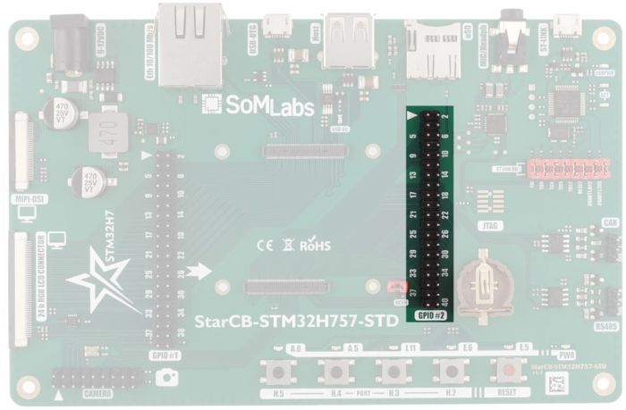
| Pin | Signal | Description |
|---|---|---|
| 1 | VDD-3V3 | Power supply for external loads (up to 200 mA1) |
| 2 | GND | - |
| 3 | UART2X.TXD | - |
| 4 | UART2X.RXD | - |
| 5 | UART2X.RTS | - |
| 6 | UART2X.RTS | - |
| 7 | PORTC.7 | - |
| 8 | PORTI.14 | Line connected to user Card Detect signal of J800 |
| 9 | PORTI.8 | - |
| 10 | PORTI.9 | - |
| 11 | PORTI.10 | - |
| 12 | - | - |
| 13 | - | - |
| 14 | - | - |
| 15 | CAN1.TX | Tx line of CAN interface (MCP2542FD) Connected to CAN-FD PHY interface |
| 16 | CAN1.RX | Rx line of CAM interface ((MCP2542FD) Connected to CAN-FD PHY interface |
| 17 | PORTG.9 | RxD of RS-485 interface (USART6.RX) Connected to RS-485 PHY interface |
| 18 | PORTG.14 | TxD of RS-485 interface (USART6.TX) Connected to RS-485 PHY interface |
| 19 | PORTD.7 | Data Enable (transmit enable) line of RS-485 interface Connected to RS-485 PHY interface |
| 20 | PORTB.5 | Optional Standby signal of CAN interface (MCP2542FD) Connected to CAN-FD PHY interface |
| 21 | PORTE.3 | Camera reset signal |
| 22 | PORTE.5 | Line connected to user LED D804 |
| 23 | I2C1.SDA | Audio codec control interface Pulled-upwith 2.2kOhm |
| 24 | I2C1.SCL | Audio codec control interface Pulled-upwith 2.2kOhm |
| 25 | PORTE.6 | Line connected to user LED D803 |
| 26 | PORTI.11 | Line connected to user LED D802 |
| 27 | PORTH.2 | Line connected to switch S803 |
| 28 | PORTH.3 | Line connected to switch S802 |
| 29 | PORTH.4 | Line connected to switch S801 |
| 30 | PORTH.5 | Line connected to switch S800 |
| 31 | PORTA.5 | Line connected to user LED D801 |
| 32 | PORTA.0 | Line connected to user LED D800 |
| 33 | PC2_C | - |
| 34 | PC3_C | - |
| 35 | PA0_C | - |
| 36 | PA1_C | - |
| 37 | UART7.CTS | - |
| 38 | UART7.RTS | - |
| 39 | UART7.RXD | - |
| 40 | UART7.TXD | - |
Note:
1. 200 mA is the total load value for 3.3V line
RGB display interface (J500, FPC/FFC 0.5mm)
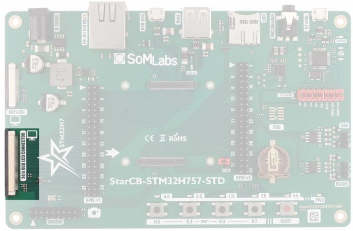
| Pin | Signal | Description |
|---|---|---|
| 1 | LCD.B0 | - |
| 2 | LCD.B1 | - |
| 3 | LCD.B2 | - |
| 4 | LCD.B3 | - |
| 5 | LCD.B4 | - |
| 6 | LCD.B5 | - |
| 7 | LCD.B6 | - |
| 8 | LCD.B7 | - |
| 9 | GND | - |
| 10 | LCD.G0 | - |
| 11 | LCD.G1 | - |
| 12 | LCD.G2 | - |
| 13 | LCD.G3 | - |
| 14 | LCD.G4 | - |
| 15 | LCD.G5 | - |
| 16 | LCD.G6 | - |
| 17 | LCD.G7 | - |
| 18 | GND | - |
| 19 | LCD.R0 | - |
| 20 | LCD.R1 | - |
| 21 | LCD.R2 | - |
| 22 | LCD.R3 | - |
| 23 | LCD.R4 | - |
| 24 | LCD.R5 | - |
| 25 | LCD.R6 | - |
| 26 | LCD.R7 | - |
| 27 | GND | - |
| 28 | LCD.DE | - |
| 29 | LCD.HSYNC | - |
| 30 | LCD.VSYNC | - |
| 31 | GND | - |
| 32 | LCD.CLK | - |
| 33 | GND | - |
| 34 | - | - |
| 35 | - | - |
| 36 | PORTB.10 | Touch-panel interrupt line, also available on connector J501 (MIPI-DSI) |
| 37 | PORTH.11 | LCD backlight PWM controller line, also available on connector J501 (MIPI-DSI) |
| 38 | - | - |
| 39 | - | - |
| 40 | - | - |
| 41 | - | - |
| 42 | I2C3.SCL | Touch-panel I2C interface, also available on connector J501 (MIPI-DSI) and J502 (Camera) and J503 (GPIO #1) With 2.2kOhm pull-up |
| 43 | I2C3.SDA | Touch-panel I2C interface, also available on connector J501 (MIPI-DSI) and J502 (Camera) and J503 (GPIO #1) With 2.2kOhm pull-up |
| 44 | GND | - |
| 45 | VDD-5V0 | +5.0V power source for LCD module |
| 46 | VDD-5V0 | +5.0V power source for LCD module |
| 47 | VDD-5V0 | +5.0V power source for LCD module |
| 48 | VDD-5V0 | +5.0V power source for LCD module |
| 49 | PORTH.6 | Touch-panel reset line, also available on connector J501 (MIPI-DSI) |
| 50 | PORTB.11 | LCD backlight on/off controller line, also available on connector J501 (MIPI-DSI) |
MIPI-DSI display interface (J501, FPC/FFC 0.5mm)
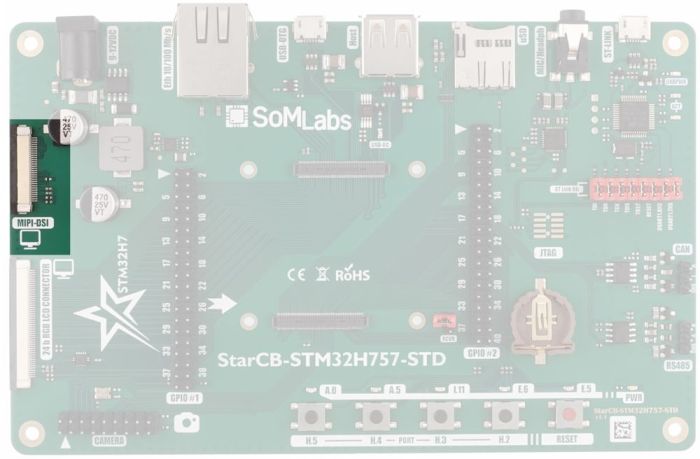
| Pin | Signal | Description |
|---|---|---|
| 1 | GND | - |
| 2 | DSI.CK_P | - |
| 3 | DSI.CK_N | - |
| 4 | GND | - |
| 5 | DSI.D0_P | - |
| 6 | DSI.D0_N | - |
| 7 | GND | - |
| 8 | DSI.D1_P | - |
| 9 | DSI.D1_N | - |
| 10 | GND | - |
| 11 | - | - |
| 12 | - | - |
| 13 | GND | - |
| 14 | - | - |
| 15 | - | - |
| 16 | GND | - |
| 17 | I2C3.SCL | Touch-panel I2C interface, also available on connector J500 (14b RGB LCD Connector) and J502 (Camera) and J503 (GPIO #1) With 2.2kOhm pull-up |
| 18 | I2C3.SDA | Touch-panel I2C interface, also available on connector J500 (14b RGB LCD Connector) and J502 (Camera) and J503 (GPIO #1) With 2.2kOhm pull-up |
| 19 | GND | - |
| 20 | PORTB.0 | LCD reset line, also available on connector J500 (14b RGB LCD Connector) |
| 21 | PORTB.10 | Touch-panel interrupt line, also available on connectors J500 (14b RGB LCD Connector) |
| 22 | PORTH.6 | Touch-panel reset line, also available on connector connector J500 (14b RGB LCD Connector) |
| 23 | GND | - |
| 24 | VDD-5V0 | +5.0V power source for LCD module |
| 25 | VDD-5V0 | +5.0V power source for LCD module |
| 26 | VDD-5V0 | +5.0V power source for LCD module |
| 27 | VDD-5V0 | +5.0V power source for LCD module |
| 28 | PORTH.11 | LCD backlight PWM controller line, also available on connector J500 (14b RGB LCD Connector) |
| 29 | PORTB.11 | LCD backlight on/off controller line, also available on connector connector J500 (14b RGB LCD Connector) |
| 30 | GND | - |
Parallel camera interface (J502, 2x9 gold-pin, 2.54mm)
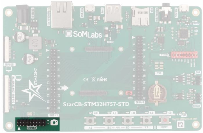
| Pin | Signal | Description |
|---|---|---|
| 1 | VDD-3V3 | Power supply for external loads (up to 200 mA1) |
| 2 | GND | - |
| 3 | I2C3.SCL | Touch-panel I2C interface, also available on connectors J500 (14b RGB LCD Connector) and J501 (MIPI-DSI) and J503 (GPIO #1) With 2.2kOhm pull-up |
| 4 | I2C3.SDA | Touch-panel I2C interface, also available on connectors J500 (14b RGB LCD Connector) and J501 (MIPI-DSI) and J503 With 2.2kOhm pull-up |
| 5 | DCAM.VSYNC | - |
| 6 | DCAM.HSYNC | - |
| 7 | DCAM.PCLK | - |
| 8 | CAM-XCLK | On-board 24 MHz clock generator |
| 9 | DCAM.D7 | - |
| 10 | DCAM.D6 | - |
| 11 | DCAM.D5 | - |
| 12 | DCAM.D4 | - |
| 13 | DCAM.D3 | - |
| 14 | DCAM.D2 | - |
| 15 | DCAM.D1 | - |
| 16 | DCAM.D0 | - |
| 17 | CAM-RST | PORTE.3 - camera reset line |
| 18 | CAM-PWD | 3.3V power supply for camera module |
Note:
1. 200 mA is the total load value for 3.3V line
2. Example recommended camera module is OV5640 Camera Breakout
CAN-FD interface (J700, 1x3 gold-pin, 2.54mm)
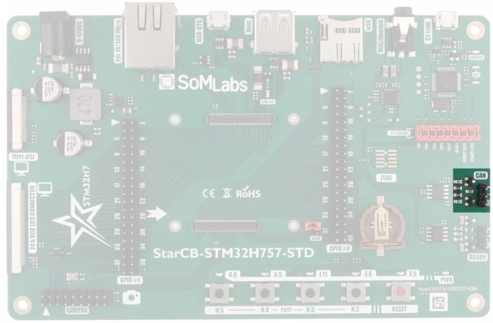
J700 connector pinout
| Pin | Signal | Description |
|---|---|---|
| 1 | GND | - |
| 2 | L | CAN L signal Line |
| 3 | H | CAN H signal Line |
CAN-FD interface connections to MCU
| Pin | Signal | Description | Note |
|---|---|---|---|
| 63 (J101) | CAN1.TX | CAN-FD Transmit Data | Connected to GPIO #2 connector |
| 61 (J101) | CAN1.TX | CAN-FD Receive Data | Connected to GPIO #2 connector |
| 53 (J101) | PORTB.5 | CAN-FD PHY layer STB signal | Connected to GPIO #2 connector |
RS-485 interface (J701, 1x3 gold-pin, 2.54mm)
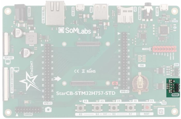
J700 connector pinout
| Pin | Signal | Description |
|---|---|---|
| 1 | GND | - |
| 2 | L | CAN L signal Line |
| 3 | H | CAN H signal Line |
CAN-FD interface connections to MCU
| Pin | Signal | Description | Note |
|---|---|---|---|
| 63 (J101) | CAN1.TX | CAN-FD Transmit Data | Connected to GPIO #2 connector |
| 61 (J101) | CAN1.TX | CAN-FD Receive Data | Connected to GPIO #2 connector |
| 53 (J101) | PORTB.5 | CAN-FD PHY layer STB signal | Connected to GPIO #2 connector |
Audio codec (J600, MiniJack)
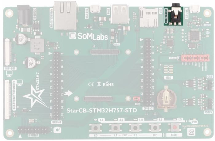
| Pin | Signal | Description | Note |
|---|---|---|---|
| 98 (J101) | I2S2.MCK | NAU88C22YG codec signal | - |
| 90 (J101) | I2S2.CK | NAU88C22YG codec signal | - |
| 88 (J101) | I2S2.WS | NAU88C22YG codec signal | - |
| 94 (J101) | I2S2.SDO | NAU88C22YG codec signal | - |
| 92 (J101) | I2S2.SDI | NAU88C22YG codec signal | - |
| 35 (J101) | I2C1.SCL | NAU88C22YG control interface | Connected to GPIO #2 connector |
| 37 (J101) | I2C1.SDA | NAU88C22YG control interface | Connected to GPIO #2 connector |
Ethernet interface (J302, RJ-45)
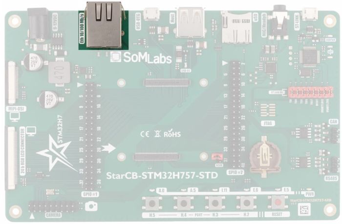
| Pin | Signal | Description | Note |
|---|---|---|---|
| 65 (J100) | ETH.TX_p | J302 TD+ pin 1 | 10/100 Mb Ethernet connector |
| 67 (J100) | ETH.TX_n | J302 TD- pin 2 | 10/100 Mb Ethernet connector |
| 71 (J100) | ETH.RX_p | J302 RD+ pin 3 | 10/100 Mb Ethernet connector |
| 73 (J100) | ETH.RX_n | J302 RD- pin 6 | 10/100 Mb Ethernet connector |
| 59 (J100) | ETH.LED0 | Green LED | - |
| 61 (J100) | ETH.LED1 | Yellow LED | - |
SD card interface (J800)
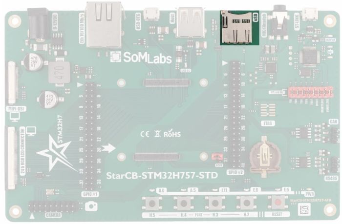
| Pin | Signal | Description | Note |
|---|---|---|---|
| 89 (J101) | SDMMC.D0 | - | - |
| 87 (J101) | SDMMC.D1 | - | - |
| 97 (J101) | SDMMC.D2 | - | - |
| 95 (J101) | SDMMC.D3 | - | - |
| 91 (J101) | SDMMC.CK | - | - |
| 93 (J101) | SDMMC.CMD | - | - |
| 93 (J101) | SDMMC.CD | Card detect signal | Connected to PORTI.14 GPIO line Available on GPIO #2 connector |
User switches
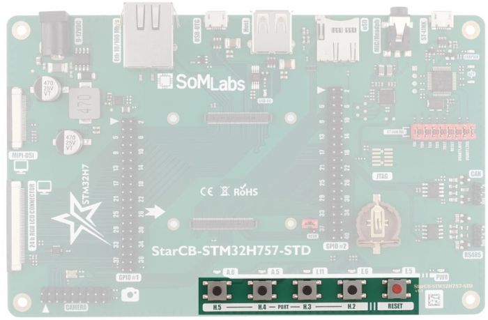
| Pin | Signal | Description | Note |
|---|---|---|---|
| 17 (J101) | H.5 | Connected to PORTH.5 | User switch |
| 19 (J101) | H.4 | Connected to PORTH.4 | User switch |
| 21 (J101) | H.3 | Connected to PORTH.3 | User switch |
| 23 (J101) | H.2 | Connected to PORTH.2 | User switch |
| 8 (J101) | RESET | Manual reset switch | Connected to JTAG connector and ST-Link debugger MCU reset line |
User LEDs
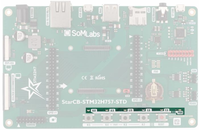
| Pin | Signal | Description | Note |
|---|---|---|---|
| 17 (J101) | A.0 | Connected to PORTA.0 | User LED, actve "0" |
| 19 (J101) | A.5 | Connected to PORTA.5 | User LED, actve "0" |
| 21 (J101) | I.11 | Connected to PORTI.11 | User LED, actve "0" |
| 23 (J101) | E.6 | Connected to PORTE.6 | User LED, actve "0" |
| 39 (J101) | E.5 | Connected to PORTE.5 | User LED, actve "0" |
| - | PWR | 3.3V power signalling | Permanantly connected to 3.3V |
Power supply connector (J200, 9-12 VDC)
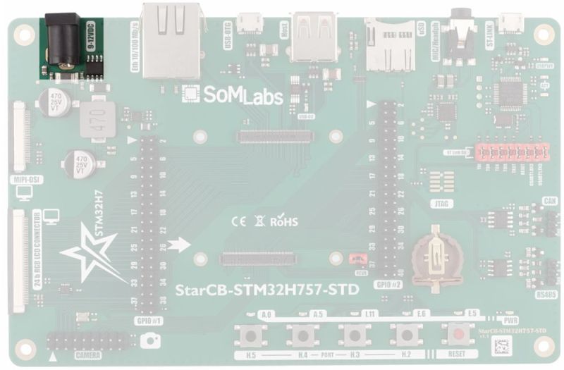
Note:
1. External power connector type DC-140-B05-00-PN (5.5/2.5 mm)
Dimensions
