VisionSOM-STM32MP1 Datasheet and Pinout: Difference between revisions
From SomLabs Wiki
| Line 213: | Line 213: | ||
|} | |} | ||
Note: <br /> | Note: <br /> | ||
1. Maximum MPU junction temperature is + | 1. Maximum MPU junction temperature is +125<sup>o</sup>C (industrial version) or +95<sup>o</sup>C (consumer version).<br /> | ||
== Electrical parameters == | == Electrical parameters == | ||
Revision as of 13:13, 9 December 2019

VisionSOM-STM32MP1 Datasheet and Pinout
General description
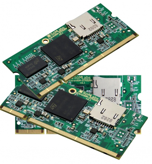
The VisionSOM-STM32MP1 family is a SODIMM-sized SoM based on the STMicroelectronics STM32MP1 application processor which features an advanced implementation of a single or dual ARM Cortex-A7 cores (at speed up to 650MHz) and ARM Cortex-M4 core (at speed up to 209MHz) as well as a 3D Graphics Processing Unit (GPU) Open GL 2.0 ES compatible.
The VisionSOM-STM32MP1 is a general-purpose highly integrated SoM (System on Module) featuring high computation power and 802.11b/g/n Wi-Fi and Bluetooth v4.1 connectivity. The option of integrated, fully certified Wi-Fi and Bluetooth module simplifies the carrier board design and is ideally suited for wireless application. The VisionSOM-STM32MP1 provides a variety memory configuration including flexible range of DDR3L, eMMC and SD memory card that meets our customers requirements.
The SoM supports connections to a variety of interfaces: two high-speed USB on-the-go with PHY, dual Ethernet, audio, display with touch panel and serial interfaces. In addition, the system supports industrial grade embedded applications.
SoMLabs also provides a complete hardware and software development board for the SoM in the form of a carrier board and optional TFT display and touch panel.
Applications
- Industrial embedded Linux computer
- Home Appliances
- Home Automation – Smart Home
- Human-machine Interfaces (HMI)
- Point-of-sales (POS) terminals
- Cash Register
- 2D barcode scanners and printers
- Smart grid infrastructure
- IoT gateways
- Residential gateways
- Machine vision equipment
- Robotics
- Fitness/outdoor equipment
Features
- Powered by STMicroelectronics STM32MP1 application processor
- Single or dual ARM Cortex-A7 cores at speed up to 650MHz
- ARM Cortex-M4 core at speed up to 209MHz
- Up to 512MB SDRAM DDR3L
- Up to 32GB eMMC memory or uSD memory card
- Optional Murata 802.11b/g/n Wi-Fi and Bluetooth v4.2+EDR module
- Power-efficient and cost-optimized solution
- Ideal for industrial IoT and embedded applications
- Integrated security features
Pictures of SOM versions
| Version | Photo |
|---|---|
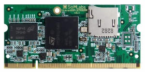
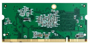
| eMMC |
  |
| micro-SD |
  |
| WiFi/BT module is available for all memory variants configurations. |
Ordering info
| SLS | Product type SLS - System on Module |
| 1 | SOM Name 1 - VisionSOM SODIMM200 |
| 8 | CPU Family 8 - STM32MP1 |
| CpuType | CPU Type MP151A - STM32MP151A MP157A - STM32MP157A |
| Clock | CPU Clock Speed 650C - 650MHz |
| RamSize | DDR3 RAM Size 256R - 256MB 512R - 512MB |
| FlashSize | Flash Size Type and Density SD - MicroSD connector 04GE - 4GB eMMC 08GE - 8GB eMMC 16GE - 16GB eMMC 32GE - 32GB eMMC |
| SF | Special Features 0SF - No Special Features 1WB - Built-in 802.11b/g/n Wi-Fi and Bluetooth v4.2+EDR Module (Murata 1DX) |
| TEMP | Operating Temperature C - Consumer: 0 to +70 C SI - Extended: -30 to +70 C I - Industrial: -40 to +85 C |
| V | SOM Version A - Version 2.1 |
Block Diagram
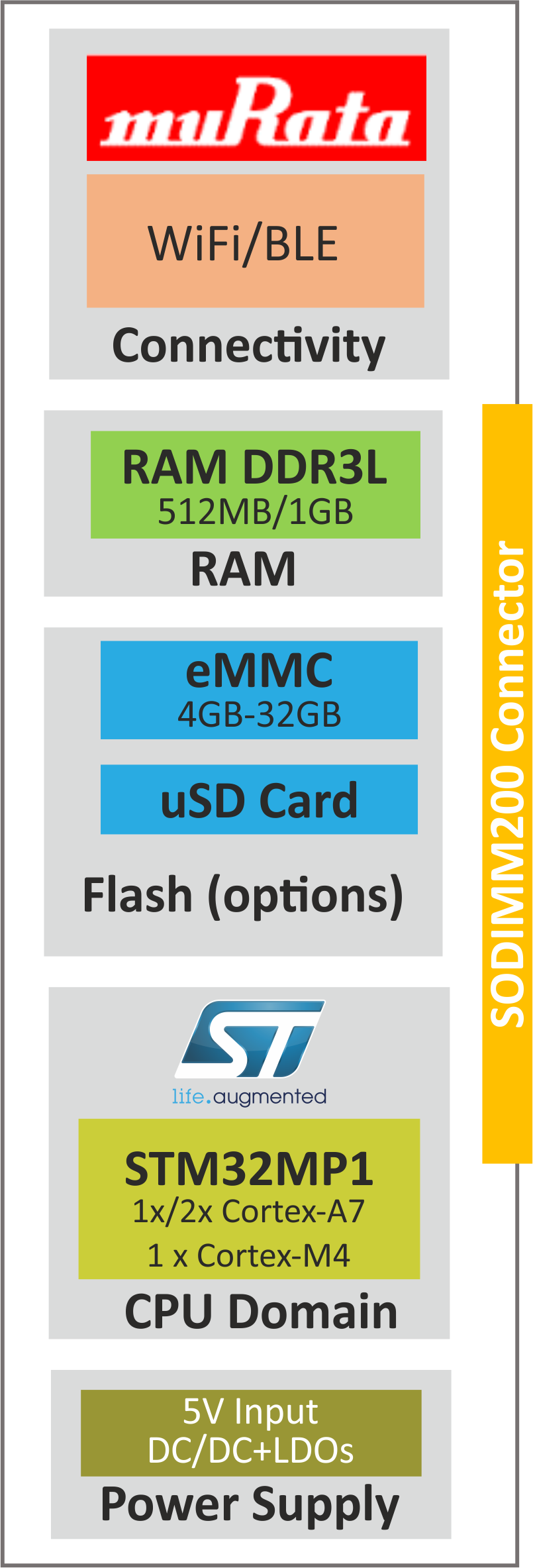
Operating ranges
| Parameter | Value | Unit | Comment |
|---|---|---|---|
| Power Supply | Connected to +5VIN SODIMM pin | ||
| Input GPIO voltage | - | ||
| Environment temperature1 | oC | Industrial range w/o WiFi module | |
| Industrial range with WiFi module | |||
| Consumer range |
Note:
1. Maximum MPU junction temperature is +125oC (industrial version) or +95oC (consumer version).
Electrical parameters
| SOM signal name |
Parameter | Value | Units | ||
|---|---|---|---|---|---|
| Min. | Typ. | Max. | |||
| +5VIN | Supply Voltage | 4.0 | 5.0 | 5.5 | V |
| - | Total Supply Current1 | x | x | x | A |
| VGPIO | GPIO Input Voltage | 0 | 3.3 | 3.62 | V |
| +3.3VOUT | SOM Internal LDO Output Current |
- | - | 0.5 | A |
| USB-OTGx-VBUS | USB Supply | 4.40 | - | 5.5 | V |
| VDD-COIN-3V | SNVS Backup Battery Supply |
2.66 | - | 3.6 | V |
| - | ADC Inputs Voltage | 0 | - | 3.3 | V |
Notes:
1. Excluding external load connected to +3.3VOUT lines.
2. Applying the maximum voltage 3.6V results in shorten lifetime. Recommended value is smaller than 3.5V.
SoM pinout
Important notes
1. Detail pin configurations description you can find, edit and arrange in dedicated MEX files (with free "i.MX Pin Tool" configurational tool):
VisionSOM-6ULL without WiFi module and no SDIO1 on edge connector or
VisionSOM-6ULL without WiFi module and with SDIO1 on edge connector or
VisionSOM-6ULL witht WiFi module on-board.
2. LCD_DATAxx pins are internally used for boot sequence configuration. We recommend to use LCD_DATAxx lines as outputs or using eFuse boot configuration.
| SODIMM PIN | GPIO name | Default function | Notes |
| 1 | GND | ||
| 2 | GND | ||
| 3 | PWR-LP | ||
| 4 | STM32-NRST | MPU reset in + on-board SD card power rail off | |
| 5 | PWR-ON | ||
| 6 | VDD-3V3 | MPU VDD power rail (for BOOT lines voltage reference only) | |
| 7 | BOOT1 | ||
| 8 | VDD-COIN-3V | External 3V battery input (optionally) | |
| 9 | BOOT0 | ||
| 10 | BOOT2 | ||
| 11 | USB-OTG1-VBUS | Analog USB interface line | |
| 15 | GND | ||
| 17 | GND | ||
| 19 | USB-OTG1-DP | Analog USB interface line | |
| 20 | GND | ||
| 21 | USB-OTG1-DN | Analog USB interface line | |
| 22 | GND | ||
| 23 | GND | ||
| 25 | USB-OTG2-DP | Analog USB interface line | |
| 26 | GND | ||
| 27 | USB-OTG2-DN | Analog USB interface line | |
| 28 | GND | ||
| 29 | GND | ||
| 35 | GND | ||
| 38 | GND | ||
| 40 | GND | ||
| 41 | GND | ||
| 43 | JTAG-TDI | JTAG interface | |
| 45 | PG10 | GPIO-PG10 | |
| 46 | JTAG-TMS | JTAG interface | |
| 47 | PC3 | GPIO-PC3-ADC1-13 | |
| 48 | JTAG-nRST | JTAG interface | |
| 49 | PD13 | GPIO-PD13 | |
| 50 | GND | ||
| 51 | GND | ||
| 52 | JTAG-TDO | JTAG interface | |
| 53 | PC1 | ENET1-MDC | |
| 54 | JTAG-TCK | JTAG interface | |
| 55 | PC0 | GPIO-PC0-ADC1-10 | |
| 56 | PB7 | GPIO-PB7 | By default I2C4_SDA |
| 57 | PE1 | UART8-TXD | |
| 58 | PB1 | GPIO-PB1-ADC1-5 | |
| 59 | GND | ||
| 60 | GND | ||
| 61 | PA2 | ENET1-MDIO | |
| 62 | PA0 | GPIO-PA0-ADC1-16 | |
| 63 | PE0 | UART8-RXD | |
| 64 | PF10 | GPIO-PF10 | |
| 65 | PD8 | USART3-TXD | |
| 66 | PD14 | UART8-CTS | |
| 67 | PD9 | USART3-RXD | |
| 68 | PG9 | USART6-RXD | |
| 69 | PA10 | USART1-RXD | |
| 70 | GND | ||
| 71 | GND | ||
| 72 | PD11 | USART3-CTS | |
| 73 | PB6 | USART1-TXD | |
| 74 | PG7 | UART8-RTS | |
| 75 | PG11 | UART4-TXD | |
| 76 | PA11 | USART1-CTS | |
| 77 | PB2 | UART4-RXD | |
| 78 | PD12 | USART3-RTS | |
| 79 | PG14 | USART6-TXD | |
| 80 | PA12 | USART1-RTS | |
| 81 | GND | ||
| 82 | GND | ||
| 84 | GND | ||
| 85 | VOUT-3V3 | 3,3V out | |
| 87 | VOUT-3V3 | 3,3V out | |
| 88 | VOUT-3V3 | 3,3V out | |
| 89 | VOUT-3V3 | 3,3V out | |
| 90 | VOUT-3V3 | 3,3V out | |
| 91 | VOUT-3V3 | 3,3V out | |
| 92 | VOUT-3V3 | 3,3V out | |
| 93 | VOUT-3V3 | 3,3V out | |
| 96 | VDD-5V | 5V input | |
| 97 | PC4 | ENET1-RXD0 | |
| 98 | VDD-5V | 5V input | |
| 99 | PC5 | ENET1-RXD1 | |
| 100 | VDD-5V | 5V input | |
| 101 | PA7 | ENET1-CRS-DV | |
| 102 | VDD-5V | 5V input | |
| 103 | GND | ||
| 104 | VDD-5V | 5V input | |
| 106 | VDD-5V | 5V input | |
| 107 | GND | ||
| 108 | VDD-5V | 5V input | |
| 109 | PG12 | GPIO-PG12 | |
| 110 | VDD-5V | 5V input | |
| 111 | PD15 | GPIO-PD15 | |
| 112 | VDD-5V | 5V input | |
| 113 | PA13 | GPIO-PA13 | |
| 114 | PB11 | ENET1-TXD-EN | |
| 115 | GND | ||
| 116 | GND | ||
| 117 | PA14 | GPIO-PA14 | |
| 118 | PB5 | ENET1-CLK | RC LPF built-in series (10R) |
| 119 | PC2 | GPIO-PC2 | |
| 120 | GND | ||
| 121 | PE2 | GPIO-PE2 | By default I2C4_SCL |
| 122 | PG13 | ENET1-TXD0 | |
| 124 | PB13 | ENET1-TXD1 | |
| 125 | GND | ||
| 127 | GND | ||
| 128 | GND | ||
| 129 | PA9 | LCD-R5 | |
| 130 | GND | ||
| 131 | PA8 | LCD-R6 | |
| 132 | GND | ||
| 133 | LCD-DATA17 (GND) | Internally connected to GND | |
| 134 | PE15 | LCD-R7 | |
| 135 | GND | ||
| 136 | GND | ||
| 137 | PC10 | LCD-R2 | |
| 138 | PB0 | LCD-R3 | |
| 139 | PF11 | LCD-G5 | |
| 140 | PA5 | LCD-R4 | |
| 141 | PC7 | LCD-G6 | |
| 142 | PG8 | LCD-G7 | |
| 143 | LCD-DATA8 (GND) | Internally connected to GND | |
| 144 | LCD-DATA16 (GND) | Internally connected to GND | |
| 145 | LCD-DATA9 (GND) | Internally connected to GND | |
| 146 | GND | ||
| 147 | GND | ||
| 148 | PE11 | LCD-G3 | |
| 149 | PA3 | LCD-B5 | |
| 150 | PB10 | LCD-G4 | |
| 151 | PB8 | LCD-B6 | |
| 152 | PA6 | LCD-G2 | |
| 153 | LCD-DATA0 (GND) | Internally connected to GND | |
| 154 | PD10 | LCD-B3 | |
| 155 | LCD-DATA1 (GND) | Internally connected to GND | |
| 156 | GND | ||
| 157 | PA1 | GPIO-PA1 | |
| 158 | PE12 | LCD-B4 | |
| 159 | GND | ||
| 160 | PC6 | LCD-HSYNC | |
| 161 | PE14 | LCD-CLK | |
| 162 | PA4 | LCD-VSYNC | |
| 163 | PE13 | LCD-DE | |
| 164 | PD6 | LCD-B2 | |
| 165 | GND | ||
| 166 | PB9 | LCD-B7 | |
| 167 | PB14 | SD2-DATA0 | |
| 168 | GND | ||
| 169 | PB4 | SD2-DATA3 | |
| 170 | GND | ||
| 171 | PB15 | SD2-DATA1 | |
| 172 | GND | ||
| 173 | PG6 | SD2-CMD | |
| 174 | GND | ||
| 175 | PB3 | SD2-DATA2 | |
| 176 | GND | ||
| 177 | GND | ||
| 178 | GND | ||
| 179 | PE3 | SD2-CLK | |
| 180 | GND | ||
| 181 | GND | ||
| 182 | GND | ||
| 184 | GND | ||
| 185 | GND | ||
| 186 | DSI-D0N | Dedicated MIPI-DSI line | |
| 188 | DSI-D0P | Dedicated MIPI-DSI line | |
| 189 | GND | ||
| 192 | DSI-D1N | Dedicated MIPI-DSI line | |
| 193 | DSI-CK-N | Dedicated MIPI-DSI line | |
| 194 | DSI-D1P | Dedicated MIPI-DSI line | |
| 195 | DSI-CK-P | Dedicated MIPI-DSI line | |
| 199 | GND | ||
| 200 | GND | ||
| - | PA15 | SD1-DATA5 | Internal Flash/SD |
| - | PB12 | WLAN-HWAKE | |
| - | PC8 | SD1-DATA0 | Internal Flash/SD |
| - | PC9 | SD1-DATA1 | Internal Flash/SD |
| - | PC11 | SD1-DATA3 | Internal Flash/SD |
| - | PC12 | SD1-CLK | Internal Flash/SD |
| - | PC13 | 32kHz-OUT | 1DX WiFi module line |
| - | PC14 | OSCI | |
| - | PC15 | OSCO | |
| - | PD0 | SD3-CMD | 1DX WiFi module line |
| - | PD1 | SD3-DATA0 | 1DX WiFi module line |
| - | PD4 | SD3-DATA1 | 1DX WiFi module line |
| - | PD5 | SD3-DATA2 | 1DX WiFi module line |
| - | PD7 | SD3-DATA3 | 1DX WiFi module line |
| - | PE4 | SD1-DATA4 | Internal Flash/SD |
| - | PE5 | SD1-DATA6 | Internal Flash/SD |
| - | PE6 | SD1-DATA2 | Internal Flash/SD |
| - | PE9 | BT-ENABLE | 1DX Bluetooth module line |
| - | PE10 | UART7-CTS | 1DX Bluetooth module line |
| - | PF6 | BT-HWAKE | 1DX Bluetooth module line |
| - | PF7 | BT-WAKE | 1DX Bluetooth module line |
| - | PF8 | UART7-RTS | 1DX Bluetooth module line |
| - | PF9 | WLAN-ENABLE | 1DX WiFi module line |
| - | PG15 | SD3-CLK | 1DX WiFi module line |
| PD2 | SD1-CMD | Internal Flash/SD | |
| PD3 | SD1-DATA7 | Internal Flash/SD | |
| PE7 | UART7-RXD | 1DX Bluetooth module line | |
| PE8 | UART7-TXD | 1DX Bluetooth module line |
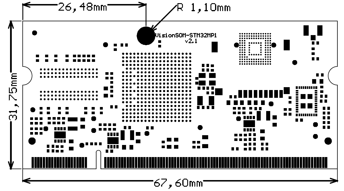
Dimensions
