SL-ADP-PCIe-M2 Datasheet and Pinout: Difference between revisions
From SomLabs Wiki
| Line 20: | Line 20: | ||
== Pictures == | == Pictures == | ||
Note: the SSD module shown in the picture is not included in the SL-ADP-PCIe-M2 kit! | |||
[[File:SL-ADP-PCIe-M2-2.jpg|800px|center]]<br> | [[File:SL-ADP-PCIe-M2-2.jpg|800px|center]]<br> | ||
[[File:SL-ADP-PCIe-M2-3.jpg|800px|center]]<br> | [[File:SL-ADP-PCIe-M2-3.jpg|800px|center]]<br> | ||
Revision as of 10:34, 4 May 2021

SL-ADP-PCIe-M2 M.2 PCIe mass storage adapter Datasheet and Pinout
General description
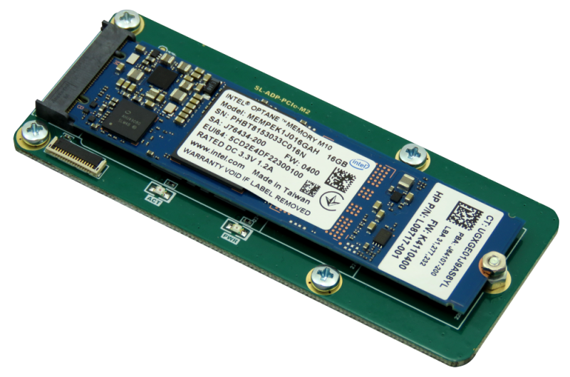
SL-ADP-PCIe-M2 is adapter dedicated to using M.2 mass storage (SSD) in embedded systems based on i.MX8Mmini.
The SL-ADP-PCIe-M2 module is equipped with FPC16 connector - the same like in SoMLabs carrier board VisionCB-8M-STD.
Features
- Equipped with M.2 key M SSD socket
- Single rail +3.3V power supply
- SSD configuration via I2C
- Dual lane PCIe communication interface
- Operating temperature -30÷+85°C
- Fully compatible with SoMLabs carrier boards equippped with PCIe interface on FPC16 connector
- Built-in 32kHz clock source
- Built-in two LEDs
- Compatible with 2242, 2260 and 2280 modules
- Connection with carrier board using FPC16 cable
Pictures
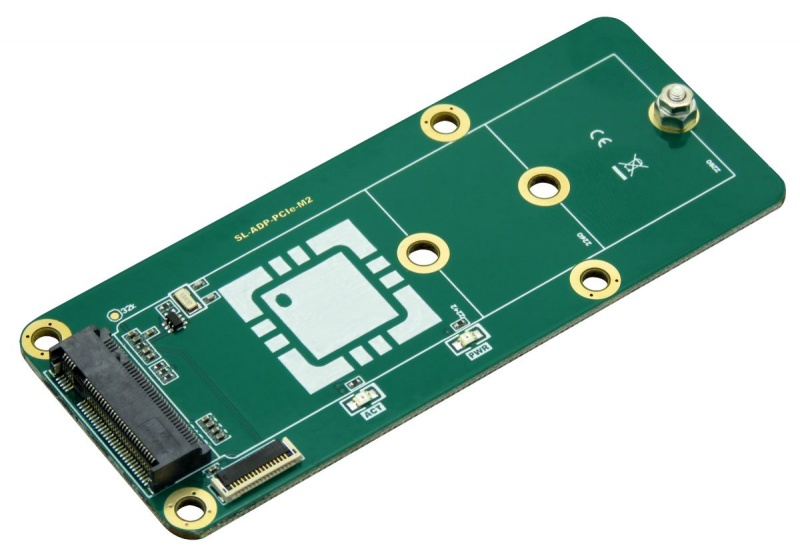
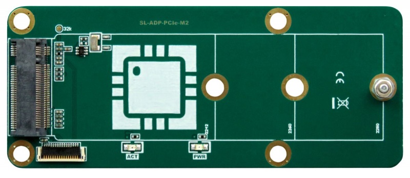
Note: the SSD module shown in the picture is not included in the SL-ADP-PCIe-M2 kit!
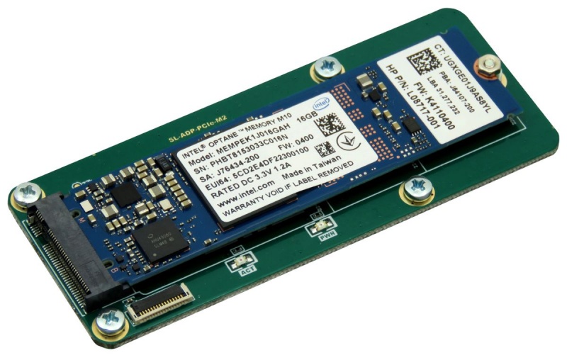
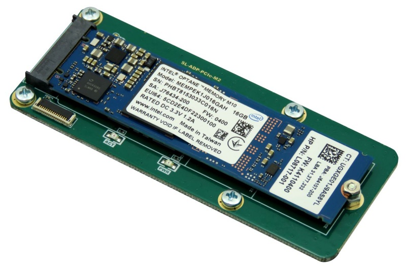
Ordering info
SL-MIPI-CSI-OV5640 - FPC 30-pin flat cable (A-A) is included.
Operating ranges
| Parameter | Value | Unit | Comment |
|---|---|---|---|
| Power Supply | Powered from carrier board | ||
| Current | Maximum peak value | ||
| Working temperature | oC | - |
Electrical parameters
| Signal name | Parameter | Value | Units | ||
|---|---|---|---|---|---|
| Min. | Typ. | Max. | |||
| +3.3V | Supply Voltage | 3.2 | 3.3 | 3.35 | V |
| I3.3V | Supply Current (3.3V) | 0.11 | .16 | - | mA |
| tPWRSEQ | PMIC power-up time | - | 150 | - | ms |
| VIO | I2C, RES, PWDN Input Voltage | 0 | 3.3 | 3.5 | V |
| fI2C | I2C Controller Speed | - | - | 400 | kHz |
| RI2C | I2C IOs Pull-up Resistance | - | 10 | - | kΩ |
| RPWDN | Serial resistors voltage divider connected between FPC30 pin and PWDN input of OV5640 sensor | - | 2x10 | - | kΩ |
MIPI-CSI (output) Pinout
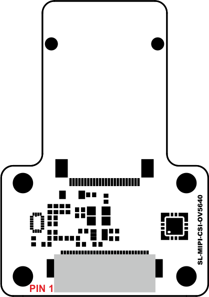
| FPC30 connector pin | Function name | Description |
|---|---|---|
| 1 | GND | - |
| 2 | - | - |
| 3 | - | - |
| 4 | - | - |
| 5 | - | - |
| 6 | +3.3V | Power supply |
| 7 | +3.3V | Power supply |
| 8 | GND | - |
| 9 | - | - |
| 10 | PWDN | OV5640 - Power Down input (active high, internal pull-down) |
| 11 | RESET | OV5640 - Reset input (active low, internal pull-up) |
| 12 | GND | - |
| 13 | SIOD_C | SDA line of configuration I2C interface (internal pull-up) |
| 14 | SIO_D | SCL line of configuration I2C interface (internal pull-up) |
| 15 | GND | - |
| 16 | - | - |
| 17 | - | - |
| 18 | GND | - |
| 19 | - | - |
| 20 | - | - |
| 21 | GND | - |
| 22 | MDN1 | CSI_DATA1_n |
| 23 | MDP1 | CSI_DATA1_p |
| 24 | GND | - |
| 25 | MDN0 | CSI_DATA0_n |
| 26 | MDP0 | CSI_DATA0_p |
| 27 | GND | - |
| 28 | MCN | CSI_CLK_n |
| 29 | MCP | CSI_CLK_p |
| 30 | GND | - |
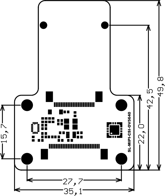
Dimensions
