SpaceCB-8Mplus-ADV Datasheet and Pinout: Difference between revisions
From SomLabs Wiki
| Line 142: | Line 142: | ||
<br>5. The I2C4 interface is common to MIPI-CSI2 and LVDS1 interfaces. | <br>5. The I2C4 interface is common to MIPI-CSI2 and LVDS1 interfaces. | ||
<br>6. The I2C6 interface supports PI5USB30213A USB-C interface controller. | <br>6. The I2C6 interface supports PI5USB30213A USB-C interface controller. | ||
<br>7. All default I2C interface lines (both: SDA and SCL of I2C1, I2C2 and | <br>7. All default I2C interface lines (both: SDA and SCL of I2C1, I2C2, I2C3 and I2C4) have pull-up resistors (4.7kOhm). | ||
<br>8. User LEDs and System LED are connected to MPU using buffers with logical inverters. | <br>8. User LEDs and System LED are connected to MPU using buffers with logical inverters. | ||
Revision as of 11:38, 15 March 2023

SpaceCB-8Mplus-ADV v.1.1 Datasheet and Pinout
General description
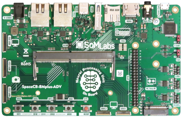
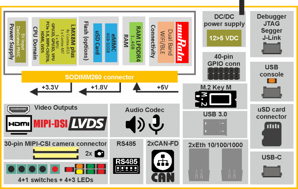
SpaceCB-8Mplus-ADV is a carrier board for the SpaceSOM-8Mplus family of computer-on-modules which are powered by NXP SOC iMX8Mplus (quad core ARM Cortex-A53+ single Cortex-M7 + Neural Processing Unit). A carrier board, together with a System on Module (SoM), makes a complete development platform similar to SBC. The carrier board houses the most common interfaces such as USB 3.0, USB-C, dual gigabit Ethernet, HDMI, PCIe, etc. A large variety of interfaces allows to use it as both a complete development platform or as a stand-alone end-product.
The carrier board connects with the SoM via a standard SODIMM connector.
SpaceCB-8Mplus-ADV carrier board is equipped with HDMI + LVDS + MIPI-DSI video outputs, 24-bit audio codec, PCIe 3.0 (M.2 key M) socket (2242, 2260, 2280), RS-485 and CAN-FD interfaces.
SpaceCB-8Mplus-ADV carrier board is equipped with Segger J-Link debugger and Linux serial console port on USB vCOM.
Applications
- AI and ML applications
- Machine vision equipment
- Robotics
- Human-machine Interfaces (HMI)
- Multimedia
- Video streaming
- Industrial embedded Linux computer
- Home Automation – Smart Home
- IoT gateways
- Residential gateways
Features
- Carrier Board (Base Board) compatible with the SpaceSOM-8Mplus family of modules based on quad core, heterogenous NXP iMX8Mplus application processors
- SoM Interface: SODIMM260
- Debug Interface: built-in Segger J-Link JTAG debugger
- Expansion Connectors:
- Serial communication/GPIO connector 2x8 Pin Header (Male)
- MicroSD card socket
- Communication Connectors:
- PCIe 3.0 (single lane, M.2 key M socket)
- RS-485 (simplex, 3 pin 2.54mm connector)
- 2x CAN-FD (3 pin 2.54mm connector)
- 2x Ethernet 10/100/1000Mbit/s, RJ45
- 1x USB Host 3.0
- 1x USB C
- 1x Console + JTAG MicroUSB B connector
- Display Interface:
- 1x HDMI
- 1x MIPI-DSI (FFP/FPC30)
- 2x LVDS (FFP/FPC22)
- Camera Interface:
- 2x MIPI-CSI2 (FFC/FPC30)
- User Interface:
- 24-bit audio codec
- Line and microphone inputs
- Speaker or headphone outputs
- 4+1 Pushbuttons
- 4+3 LEDs
- External Power Supply 9-12V DC
- Temperature Range: 0 to +70°C
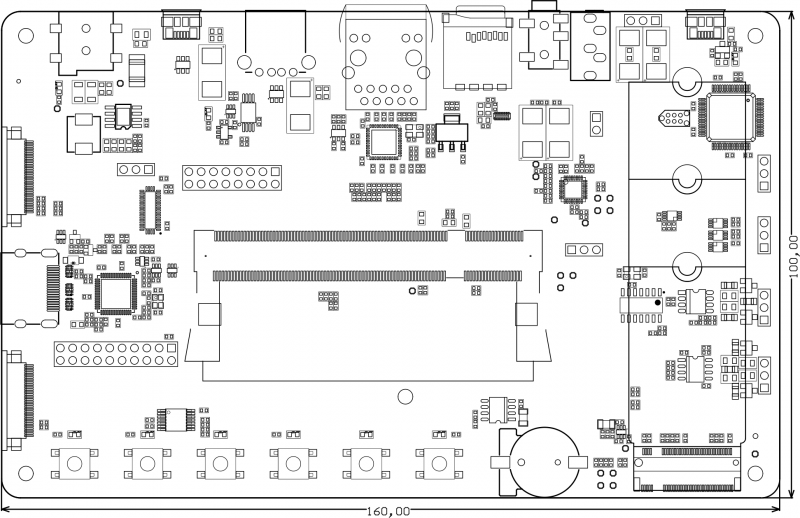
- Board Size: 160mm x 100mm x 25mm
Pictures of SpaceCB-8Mplus-ADV v1.1 board
| Version | Photo |
|---|---|
| SpaceCB-8Mplus-ADV v1.1 board only |
 |
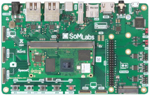
| SpaceCB-8Mplus-ADV v1.1 with SpaceSOM-8Mplus |
 |
| SpaceCB-8Mplus-ADV with SpaceSOM-8Mplus and M.2 SSD drive |
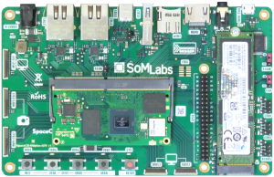 |
Ordering info
Block Diagram
Electrical parameters
| Parameter | Value | Units | Comment | ||
|---|---|---|---|---|---|
| Min. | Typ. | Max. | |||
| Power Supply | 9.0 | 12.0 | 15.0 | V | Positive pole on central connector of J101 |
| Supply current | - | - | 0.8 | A | Excluding LCD, USB and another external loads |
| MIPI-DSI Power Supply (logic) | 3.25 | 3.3 | 3.35 | V | - |
| MIPI-DSI Power Supply (backlight and aux) | 4.85 | 5 | 5.1 | V | - |
| LVDS Power Supply (aux, up to 100mA) |
4.85 | 5 | 5.1 | V | - |
Important information
1. The SpaceCB-8M-ADV carrier board is equippped with dual triple-speed 10/100/1000Mb/s Ethernet interface - RTL812F. Chips are connected to MPU using RGMII interface.
2. The I2C1 interface is common to MIPI-DSI, MIPI-CSI1 and LVDS2 interfaces.
3. The I2C2 interface is common to audio codec, .
4. The I2C3 interface supports touch-panel controller connected to MIPI-DSI interface (J502).
5. The I2C4 interface is common to MIPI-CSI2 and LVDS1 interfaces.
6. The I2C6 interface supports PI5USB30213A USB-C interface controller.
7. All default I2C interface lines (both: SDA and SCL of I2C1, I2C2, I2C3 and I2C4) have pull-up resistors (4.7kOhm).
8. User LEDs and System LED are connected to MPU using buffers with logical inverters.
M.2 socket - key M (PCIe interface, J100)
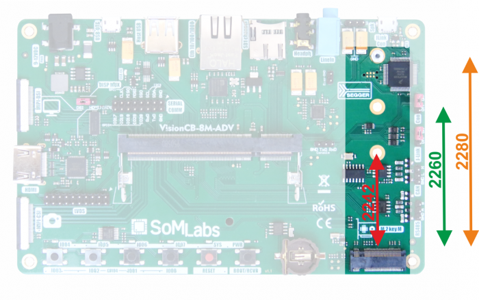
| Default MPU pin name | M.2 line |
|---|---|
| GPIO4_IO11 | PEWAKE# |
| GPIO4_IO12 | CLKREQ# |
| GPIO4_IO13 | PERST# |
| GPIO4_IO14 | DEVSLP |
Note:
1. IO[14..11] are used optionally.
2. Implemented PCIe is single lane interface.
3. M.2 socket is key M type.
4. By default CONFIG[3..0]=1111b.
Camera MIPI-CSI interface (J301, FPC/FFC 0.5mm)
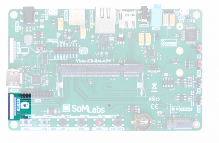
| Pin | Default MPU pin name | MPU pin | Description |
|---|---|---|---|
| 1 | GND | - | - |
| 2 | CSI-CLK-P | - | - |
| 3 | CSI-CLK-P | - | - |
| 4 | GND | - | - |
| 5 | CSI-DATA0-P | - | - |
| 6 | CSI-DATA0-N | - | - |
| 7 | GND | - | - |
| 8 | CSI-DATA1-P | - | - |
| 9 | CSI-DATA1-N | - | - |
| 10 | GND | - | - |
| 11 | CSI-DATA2-P | - | - |
| 12 | CSI-DATA2-N | - | - |
| 13 | GND | - | |
| 14 | CSI-DATA3-P | - | - |
| 15 | CSI-DATA3-N | - | - |
| 16 | GND | - | - |
| 17 | I2C1-SCL | E9 | Confguration I2C interface with 4.7kOhm pull-up (3.3V) |
| 18 | I2C1-SDA | F9 | Confguration I2C interface with 4.7kOhm pull-up (3.3V) |
| 19 | GND | - | - |
| 20 | RES | AG19 | GPIO4-IO08 (SAI1-RXD6) |
| 21 | PWRDN | AF19 | GPIO4-IO09 (SAI1-RXD7) |
| 22 | - | - | - |
| 23 | GND | - | - |
| 24 | +3.3V | - | Power supply for external devices |
| 25 | +3.3V | - | Power supply for external devices |
| 26 | +5V | - | Power supply for external devices |
| 27 | +5V | - | Power supply for external devices |
| 28 | - | - | - |
| 29 | - | - | - |
| 30 | GND | - | - |
Note:
1. 1st pin of J301 connector is at the top of the image.
2. The I2C1 interface is common to MIPI-CSI interface and audio codec.
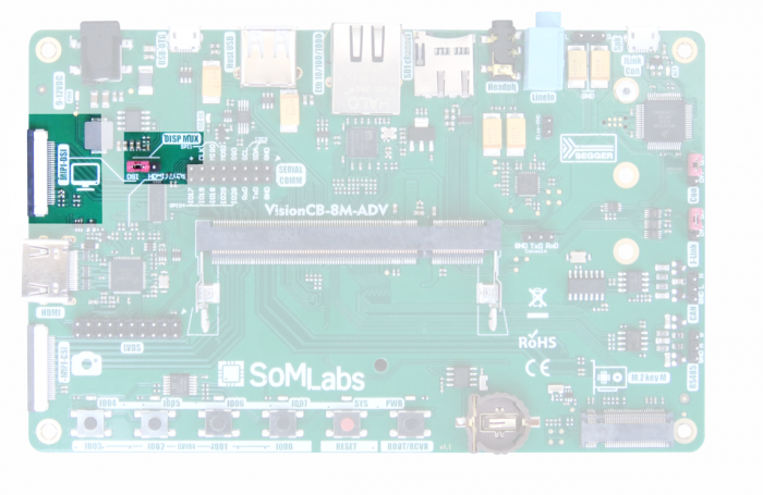
Display MIPI-DSI interface (J900, FPC/FFC 0.5mm)
| J900 pin | Default MPU pin name | MPU pin | Description |
|---|---|---|---|
| 1 | GND | - | - |
| 2 | DSI-CLK-P | - | - |
| 3 | DSI-CLK-P | - | - |
| 4 | GND | - | - |
| 5 | DSI-DATA0-P | - | - |
| 6 | DSI-DATA0-N | - | - |
| 7 | GND | - | - |
| 8 | DSI-DATA1-P | - | - |
| 9 | DSI-DATA1-N | - | - |
| 10 | GND | - | - |
| 11 | DSI-DATA2-P | - | - |
| 12 | DSI-DATA2-N | - | - |
| 13 | GND | - | |
| 14 | DSI-DATA3-P | - | - |
| 15 | DSI-DATA3-N | - | - |
| 16 | GND | - | - |
| 17 | I2C2-SCL | D10 | Display confguration I2C interface with 4.7kOhm pull-up (3.3V) |
| 18 | I2C2-SDA | D9 | Display confguration I2C interface with 4.7kOhm pull-up (3.3V) |
| 19 | GND | - | - |
| 20 | GPIO5-IO22 | E14 | MIPI-DSI display reset signal (common with MIPI-DSI>HDMI/LVDS bridge) |
| 21 | GPIO5-IO23 | F13 | Optional touch-panel interrupt signal muxed with MIPI-DSI>HDMI/LVDS bridge (with 47k pull-up) |
| 22 | SPDIF-TX | AF9 | Optional touch-panel controller reset |
| 23 | GND | - | - |
| 24 | +3.3V | - | Power supply for external devices |
| 25 | +3.3V | - | Power supply for external devices |
| 26 | +5V | - | Power supply for external devices |
| 27 | +5V | - | Power supply for external devices |
| 28 | SPDIF-RX | AG9 | Optional backlight intensity PWM controller |
| 29 | SPDIF-CLK | AF8 | Optional backlight enable |
| 30 | GND | - | - |
Note:
1. 1st pin of J900 connector is at the top of the image.
2. For configuration purposes is used I2C2 interface.
3. MIPI-DSI interface is muxed with J901 (DISP MUX) between J900 (raw MIPI-DSI output) and HDMI/LVDS converter.
4. The I2C2 interface is common to onboard RTC, HDMI-DDC, LT8912B bridge configuration and MIPI-DSI display controller.
HDMI and LVDS display interface
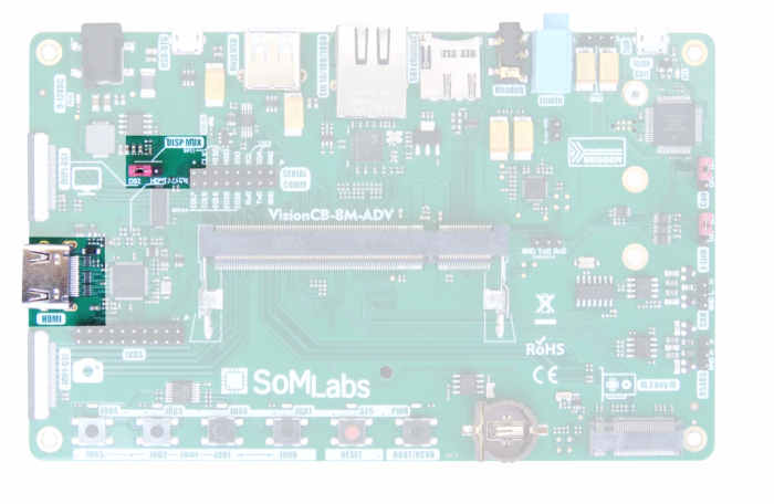
The VisionCB-8M-ADV board is equipped with MIPI-DSI > HDMI/LVDS hardware bridge (converter) based on Lontium LT8912B.
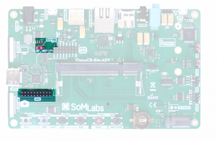
HDMI signals are available on standard HDMI connector (marked as HDMI), LVDS signals are connected to 20 pin 2.54mm 2 row connector (marked as LVDS).
The VisionCB-8M-ADV board is equipped with jumper (DISP MUX) for selecting displays: MIPI-DSI or HDMI/LVDS.
| Default MPU pin name | MPU Pin | Description |
|---|---|---|
| DSI-CLK-P | - | Signal provided to LT8912B by mux (DISP MUX, J901) |
| DSI-CLK-P | - | Signal provided to LT8912B by mux (DISP MUX, J901) |
| DSI-DATA0-P | - | Signal provided to LT8912B by mux (DISP MUX, J901) |
| DSI-DATA0-N | - | Signal provided to LT8912B by mux (DISP MUX, J901) |
| DSI-DATA1-P | - | Signal provided to LT8912B by mux (DISP MUX, J901) |
| DSI-DATA1-N | - | Signal provided to LT8912B by mux (DISP MUX, J901) |
| DSI-DATA2-P | - | Signal provided to LT8912B by mux (DISP MUX, J901) |
| DSI-DATA2-N | - | Signal provided to LT8912B by mux (DISP MUX, J901) |
| DSI-DATA3-P | - | Signal provided to LT8912B by mux (DISP MUX, J901) |
| DSI-DATA3-N | - | Signal provided to LT8912B by mux (DISP MUX, J901) |
| HDMI-DETECT | AB19 | GPIO4-IO10 (SAI1_MCLK) |
| HDMI-INT | F13 | GPIO5-IO23, signal connected to LT8912B by mux (DISP MUX, J901) |
| HDMI-RES | E14 | GPIO5-IO22 (common with MIPI-DSI reset line) |
| I2C2-SCL | D10 | Display confguration I2C interface with 4.7kOhm pull-up (3.3V) |
| I2C2-SDA | D9 | Display confguration I2C interface with 4.7kOhm pull-up (3.3V) |
| SPDIF-TX | AF9 | Audio output, signal provided to LT8912B by mux (DISP MUX, J901) |
Note:
1. The I2C2 interface is common to onboard RTC, HDMI-DDC, LT8912B bridge configuration and MIPI-DSI display controller.
2. MIPI-DSI interface is muxed with J901 (DISP MUX) between J900 (raw MIPI-DSI output) and HDMI/LVDS converter.
| J902 Pin | Signal | MPU pin |
|---|---|---|
| 1 | +5V power supply for external devices | - |
| 2 | +5V power supply for external devices | - |
| 3 | GPIO4-IO28 | AG8 (SAI3-RXFS, optional use) This pin is connected as GPIO to SERIAL COMM connector J303 |
| 4 | GPIO4-IO29 | AG7 (UART2-CTS, optional use) This pin is connected as GPIO to SERIAL COMM connector J303 |
| 5 | GND | - |
| 6 | GND | - |
| 7 | D0n | - |
| 8 | D0p | - |
| 9 | D1n | - |
| 10 | D1p | - |
| 11 | D2n | - |
| 12 | D2p | - |
| 13 | GND | - |
| 14 | GND | - |
| 15 | CLKn | - |
| 16 | CLKp | - |
| 17 | D3n | - |
| 18 | D3p | - |
| 19 | I2C2-SCL, confguration I2C interface with 4.7kOhm pull-up (3.3V) | D10 |
| 20 | I2C2-SDA, confguration I2C interface with 4.7kOhm pull-up (3.3V) | D9 |
Note:
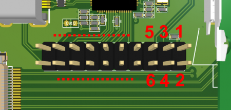
1. 1st pin of J902 connector (LVDS) is marked with arrow.
2. The I2C2 interface is common to onboard RTC, HDMI-DDC, LT8912B bridge configuration and MIPI-DSI display controller.
3. MIPI-DSI interface is muxed with J901 (DISP MUX) between J900 (raw MIPI-DSI output) and HDMI/LVDS converter.
USB and USB-OTG interfaces
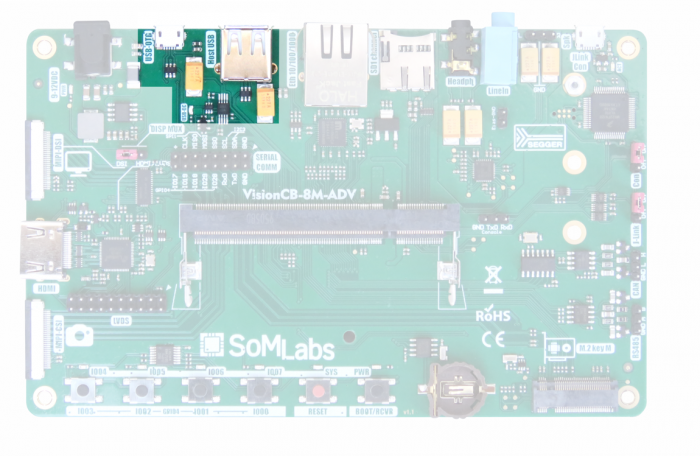
The VisionCB-8M-ADV is equipped with 2 channel of USB:
- USB-OTG (connector J501, microUSB) - connected to MPU's USB1 channel,
- host USB 2.0 (connector J501, USB-A) - connected to MPU's USB2 channel.
In both channels external USB devices are powered with power switch equipped with monitored outputs. In the event of a short circuit the LED-OC lights-up signalling overcurrent.
USB Console Port and Segger J-Link debugger
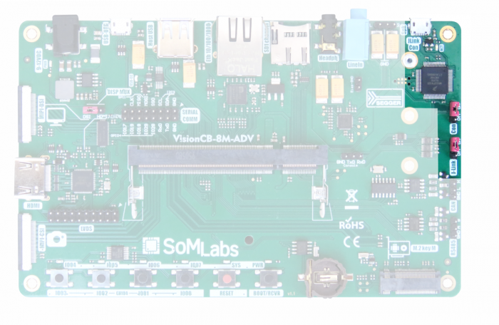
| MPU Port | Default MPU pin name | Description |
|---|---|---|
| CONSOLE-TXD | UART4-TXD | Signal connected to J304 pin 2 |
| CONSOLE-RXD | UART4-RXD | Signal connected to J304 pin 3 |
Notes:
1. Linux console port (UART4 in MPU) uses vCOM interface provided by built-in debugger Segger J-Link.
2. vCOM can be disconnected from MPU with JP801 (jumper CON in position ON or OFF).
3. Lines TXD and RXD of UART4 are easy to monitoring thanks to using J304 gold-pins.
4. Debug JTAG interface can be disconnected from MPU with JP801 (jumper J-LINK in position ON or OFF).
5. J-Link activity is monitored with ACT LED.
MicroSD card interface (J308)
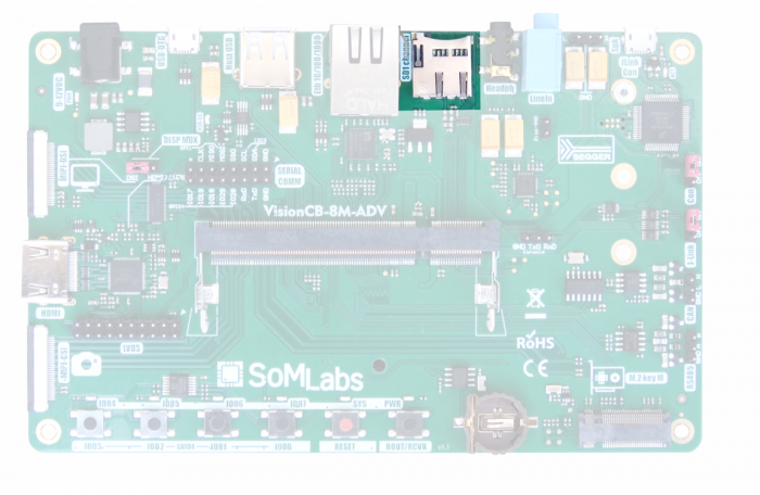
| Card connector pin | SD card signal | Default MPU pin name |
|---|---|---|
| 1 | DATA2 | SD1-DATA2 |
| 2 | DATA3 | SD1-DATA3 |
| 3 | CMD | SD1-CMD |
| 4 | NVCC-SDIO | Voltage selected 1.8/3.3V by SD1 driver |
| 5 | CLK | SD1-CLK |
| 6 | GND | - |
| 7 | DATA0 | SD1-DATA0 |
| 8 | DATA1 | SD1-DATA1 |
| 9 | CARD-DETECT | SD1-CD |
24-bit stereo audio codec
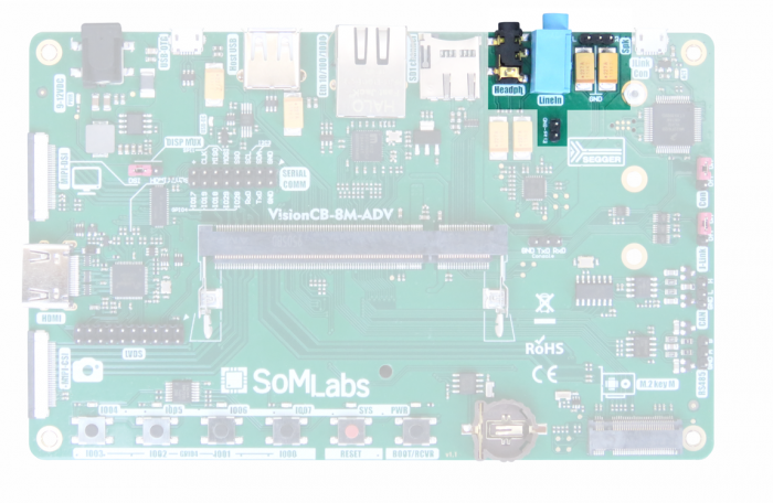
The VisionCB-8M-ADV board is equipped with 24-bit stereo codec - Nuvoton NAU88C22YG - with integrated audio amplifier.
The NAU88C22 is a low power, high quality CODEC for portable and general purpose audio applications. In addition to precision 24-bit stereo ADCs and DACs, NAU88C22YG integrates a broad range of additional functions to simplify implementation of complete audio system solutions. The NAU88C22 includes drivers for speaker, headphone, and differential or stereo line outputs, and integrates preamps for stereo differential microphones,significantly reducing external component requirements.
Connector marked Spk can be used as stereo (Left-GND/Right-GND) or mono bridge output (speaker connected to L-R pins).
| Default MPU pin name | MPU pin | Description |
|---|---|---|
| SAI3-MCLK | AD6 | Codec master clock |
| SAI3-TXC | AG6 | Codec BCLK line |
| SAI3-TXFS | AC6 | Codec FS line |
| SAI3-TXD | AF6 | Codec input line |
| SAI3-RXD | AF7 | Codec output line |
| I2C1-SCL | E9 | Confguration I2C interface with 4.7kOhm pull-up (3.3V) |
| I2C1-SDA | F9 | UConfguration I2C interface with 4.7kOhm pull-up (3.3V) |
Note:
1. The I2C1 interface is common to MIPI-CSI interface and audio codec.
On-board RTC
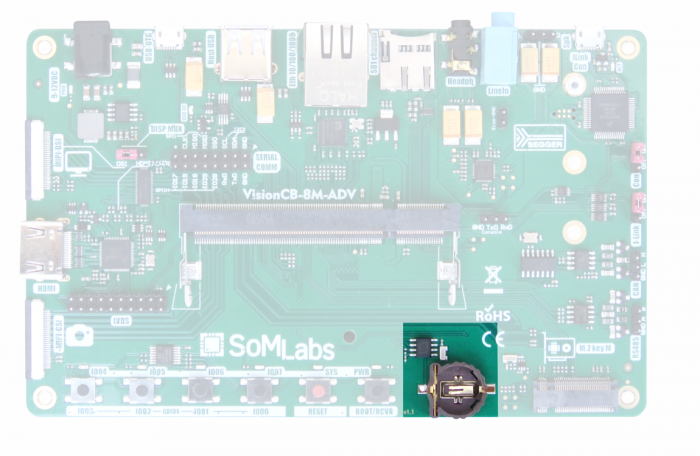
The VisionCB-8M-ADV is equipped with on-board RTC module based on NXP PCF85263AT.
The PCF85263A is a CMOS1 Real-Time Clock (RTC) and calendar optimized for low power consumption and with automatic switching to battery on main power loss.
The RTC can also be configured as a stop-watch (elapsed time counter). Three time log registers triggered from battery switch-over as well as input driven events.
Featuring clock output and two independent interrupt signals, two alarms, I2C interface and quartz crystal calibration.
RTC can be powered by an external CR1220 battery (socket J302).
| Default MPU pin name | MPU pin | Description |
|---|---|---|
| I2C2-SCL | D10 | Communication I2C interface with 4.7kOhm pull-up (3.3V) |
| I2C2-SDA | D9 | Communication I2C interface with 4.7kOhm pull-up (3.3V) |
| GPIO4-IO15 | AC6 | RTC interrupt line with 4.7kOhm pull-up (3.3V) |
Notes:
1. The I2C2 interface is common to onboard RTC, HDMI-DDC, LT8912B bridge configuration and MIPI-DSI display controller.
CAN FD serial interface
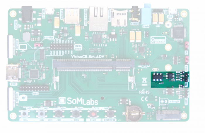
The VisionCB-8M-ADV board is equipped with Microchip CAN FD controller (MCP2518FDT-E/SL) with physical layer interface (MCP2542FD-E/SN).
The MCP2518FD supports both CAN frames in the Classical format (CAN 2.0B) and CAN Flexible Data Rate (CAN FD) format as specified in ISO11898-1:2015.
The MCP2518FD is connected to default SPI2 channel and pins.
| Signal | Default MPU pin name | Description |
|---|---|---|
| SDO | SPI2-MISO | SPI2 MISO (MCP2518FDT output) |
| SDI | SPI2-MOSI | SPI2 MOSI (MCP2518FDT input) |
| SCK | SPI2-SCK | SPI2 clock |
| CS# | SPI2-SS0 | Select MCP2518FDT device |
| INT# | GPIO4-IO16 | Interrupt from MCP2518FDT |
RS-485 simplex serial interface
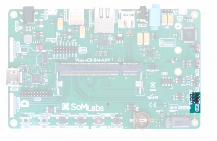
The VisionCB-8M-ADV board is equipped with low-voltage RS-485 physical layer interface MAX3485.
The RS-485 is connected to default UART3 (TxD, RxD) channel and pins. Transmission control lines (RE# and DE) are controlled by MPU hardware.
| Signal | Default MPU pin name | Description |
|---|---|---|
| RO | UART3-RXD | Data received by MPU |
| DI | UART3-TXD | Data transmitted by MPU |
| RE#/DE | SPI1-MISO | Receiver Enable (active low)/Transmitter Enable (active high) signal This signal is also connected to J303 (SERIAL COMM connector) |
Serial Communication/GPIO header (J303)
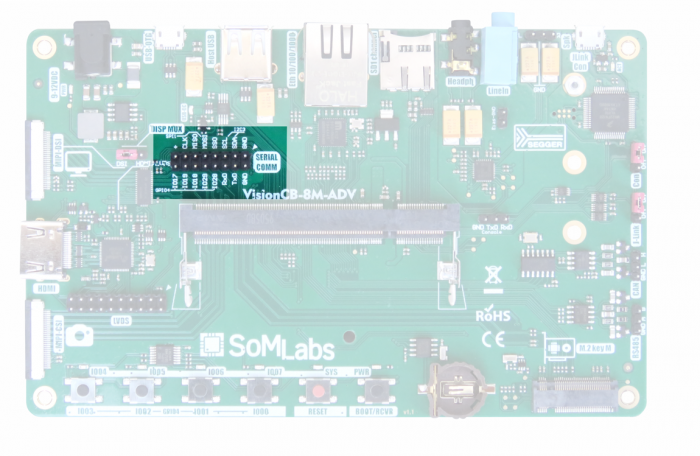
Pin numeration, 1st pin of J303 connector SERIAL COMM is marked with arrow (on picture above).
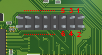
| Pin | Default pin name | Description |
|---|---|---|
| 1 | GND | - |
| 2 | GND | - |
| 3 | I2C3-SDA | By default: I2C interface with 4.7kOhm pull-up (3.3V) |
| 4 | UART2-TXD | By default: UART2-TXD or universal GPIO with 3.3V logic levels |
| 5 | I2C3-SCL | By default: I2C interface with 4.7kOhm pull-up (3.3V) |
| 6 | UART2-RXD | By default: UART2-RXD or universal GPIO with 3.3V logic levels |
| 7 | SPI1-SS0 | By default: SPI1-SS0 or universal GPIO with 3.3V logic levels |
| 8 | GPIO4-IO28 | By default: GPIO4-IO28 or universal GPIO with 3.3V logic levels Optionally can be used in LVDS channel |
| 9 | SPI1-MOSI | By default: SPI1-MOSI or universal GPIO with 3.3V logic levels |
| 10 | GPIO4-IO29 | By default: GPIO4-IO29 or universal GPIO with 3.3V logic levels Optionally can be used in LVDS channel |
| 11 | SPI1-MISO | By default: SPI1-MISO or universal GPIO with 3.3V logic levels This signal is used as RE#/DE signal in RS-485 communication channel |
| 12 | GPIO4-IO18 | By default: GPIO4-IO18 or universal GPIO with 3.3V logic levels |
| 13 | SPI1-CLK | By default: SPI1-CLK or universal GPIO with 3.3V logic levels |
| 14 | GPIO4-IO19 | By default: GPIO4-IO19 or universal GPIO with 3.3V logic levels |
| 15 | +3.3V | +3.3V generated by DC/DC built-in SOM (limited current load) |
| 16 | GPIO4-IO17 | By default: GPIO4-IO17 or universal GPIO with 3.3V logic levels |
Note:
1. 1st pin of J303 connector SERIAL COMM is marked with arrow.
User Interface (switches and LEDs)
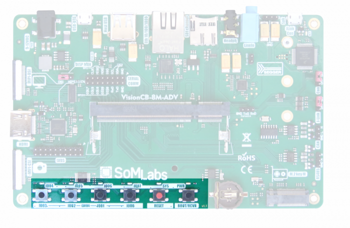
User switches
| Switch | GPIO | Description |
|---|---|---|
| S305 (black, most on the left) | GPIO4-IO03 | 47k pull-up |
| S304 | GPIO4-IO02 | 47k pull-up |
| S303 | GPIO4-IO01 | 47k pull-up |
| S302 (black, most on the right) | GPIO4-IO00 | 47k pull-up |
System switches
| Switch | Signal name | Description |
|---|---|---|
| S301 (left, red) | Reset | - |
| S300 (right) | BOOT-RECOVERY | - |
User LEDs
| LED | GPIO | Description |
|---|---|---|
| D303 (most on the left) | GPIO4-IO04 | User LED1, buffered with inverter |
| D302 | GPIO4-IO05 | User LED2, buffered with inverter |
| D301 | GPIO4-IO06 | User LED3, buffered with inverter |
| D300 (most on the right) | GPIO4-IO07 | User LED4, buffered with inverter |
System LEDs
| LED | GPIO | Description |
|---|---|---|
| D304 | SYS-LED | System function monitoring |
| D305 | - | Power LED (3.3V) |
Dimensions
