VisionSOM-RT Datasheet and Pinout: Difference between revisions
From SomLabs Wiki
| Line 267: | Line 267: | ||
{| class="wikitable" | {| class="wikitable" | ||
! style="text-align: center; font-weight:bold;" | SODIMM pin | ! style="text-align: center; font-weight:bold;" | SODIMM pin | ||
! style="text-align: center; font-weight:bold;" | | ! style="text-align: center; font-weight:bold;" | Functional domain | ||
! style="text-align: center; font-weight:bold;" | Functionname | ! style="text-align: center; font-weight:bold;" | Functionname | ||
! style="text-align: center; font-weight:bold;" | i.MX-RT | ! style="text-align: center; font-weight:bold;" | i.MX-RT pad name | ||
! style="text-align: center; font-weight:bold;" | Description (refer to i.MX-RT manuals for details) | ! style="text-align: center; font-weight:bold;" | Description (refer to i.MX-RT manuals for details) | ||
|- | |- | ||
Revision as of 12:21, 14 February 2019

VisionSOM-RT Datasheet and Pinout
General description
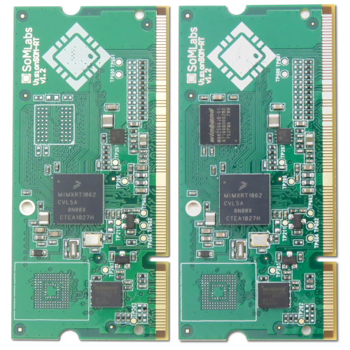
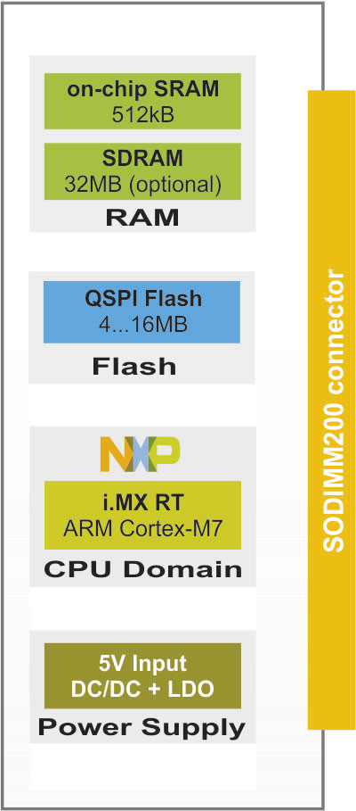
The VisionSOM-RT family is a SODIMM-sized SoM based on the NXP i.MX RT application processor which features an advanced implementation of a single ARM Cortex-M7 core (at speeds up to 600MHz).
The VisionSOM-RT is a low power highly integrated SoM (System-on-Module) featuring high computation performance, real-time functionality and MCU usability. High security enabled by AES-128, HAB and On-the-fly QSPI Flash Decryption together with 2D graphical acceleration make an ideally suited solution for home and industrial control systems, wireless application, communication solutions and real-time systems.
The system supports industrial grade targeting embedded application.
SOMLabs also provides a complete hardware and software development board for the SoM in the form of a carrier board and optional TFT display and touch panel.
Applications
- Industrial embedded RTOS computer
- Home Appliances
- Home Automation – Smart Home
- Human-machine Interfaces (HMI)
- Point-of-sales (POS) terminals
- Cash Register
- 2D barcode scanners and printers
- Smart grid Infrastructure
- IoT gateways
- Residential getaways
- Machine vision equipment
- Robotics
- Fitness/outdoor equipment
Features
- Powered by NXP i.MX RT application processor
- Core clock up to 600MHz
- 512kB on-chip RAM memory
- 256Mb (32MB) SDRAM memory
- 128Mb (16MB) QuadSPI Flash memory
- Power-efficient and cost-optimized solution
- Ideal for industrial IoT and embedded applications
- FreeRTOS support
Pictures of SOM versions
| Version | Photo |
|---|---|
| RAM&QSPI |
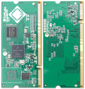 |
| QSPI |
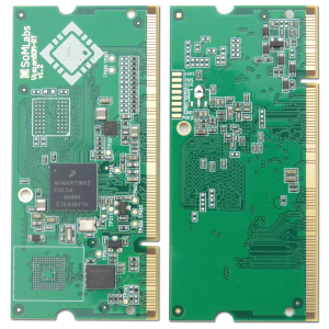 |
Ordering info
| SLS | Product type SLS - System on Module |
| N | SOM Name 1 - VisionSOM SODIMM200 |
| 2 | CPU Family 2 - i.MX RT |
| CpuType | CPU Type RT52 - i.MX RT 1052 RT62 - i.MX RT 1062 |
| Clock | CPU Clock Speed 528C - 528MHz |
| RamSize | RAM Size 0R - No RAM 32R - 32MB |
| FlashSize | Flash Size Type and Density 4QSPI - 4MB QSPI Flash 16QSPI - 16MB QSPI Flash |
| SF | Special Features 0SF - No Special Features |
| TEMP | Operating Temperature C - Consumer: 0 to +70 C I - Industrial: -40 to +85 C |
| V | SOM Version A - Version 1.2 |
Block Diagram
Operating ranges
| Parameter | Value | Unit | Comment |
|---|---|---|---|
| Power Supply | Connected to +5VIN SODIMM pin | ||
| Input GPIO voltage | - | ||
| Environment temperature1 | oC | Industrial range | |
| Consumer range |
Note:
1. Maximum MPU junction temperature is +105oC (industrial version) or +95oC (consumer version).
Electrical parameters
| SOM signal name |
Parameter | Value | Units | ||
|---|---|---|---|---|---|
| Min. | Typ. | Max. | |||
| +5VIN | Supply Voltage | 4.0 | 5.0 | 5.5 | V |
| - | Total Supply Current1 | x | x | x | A |
| VGPIO | GPIO Input Voltage | 0 | 3.3 | 3.62 | V |
| +3.3VOUT | SOM Internal LDO Output Current |
- | - | 0.5 | A |
| USB-OTGx-VBUS | USB Supply | 4.40 | - | 5.5 | V |
| VDD-COIN-3V | SNVS Backup Battery Supply |
2.66 | - | 3.6 | V |
| - | ADC Inputs Voltage | 0 | - | 3.3 | V |
Notes:
1. Excluding external load connected to +3.3VOUT lines.
2. Applying the maximum voltage 3.6V results in shorten lifetime. Recommended value is smaller than 3.5V.
Pinout
| SODIMM pin | Functional domain | Functionname | i.MX-RT pad name | Description (refer to i.MX-RT manuals for details) |
|---|---|---|---|---|
| 1 | Power | GND | - | - |
| 2 | Power | GND | - | - |
| 3 | Ctrl | PMIC-STBY-REQ | CCM_PMIC_STBY_REQ | Output, leave open if not used. |
| 4 | Ctrl | POR-B | - | External warm reset input, active L. |
| 5 | Ctrl | PMIC-ON-REQ | SNVS_PMIC_ON_REQ | Output, leave open if not used. |
| 6 | Power | VDD-SNVS-3V3 | VDD_SNVS_IN | SNVS backup power supply must be held between 2.9V and 3.3V if the system requires keeping real time and other data on OFF state. Internally connected to +3.3V, leave open. |
| 7 | BOOT | BOOT-MODE1 | GPIO_AD_B0_05 | BOOT1 configuration line or multifunction GPIO with 3.3V logic levels. |
| 8 | Power | VDD-COIN-3V | VDD_SNVS_IN | Optional external coin battery for SNVS power domain, must be held between 2.9V and 3.3V if the system requires keeping real time and other data on OFF state.Leave open if not used. |
| 9 | BOOT | BOOT-MODE0 | GPIO_AD_B0_04 | BOOT1 configuration line or multifunction GPIO with 3.3V logic levels.Pin shared with GPIO-4 line. |
| 10 | NC | - | - | Not internally connected. |
| 11 | USB | USB-OTG2-VBUS | USB_OTG2_VBUS | +5V USB bus. Leave open if not used. |
| 12 | NC | - | - | Not internally connected. |
| 13 | USB | USB-OTG1-VBUS | USB_OTG1_VBUS | +5V USB bus. Leave open if not used. |
| 14 | Ctrl | ONOFF | ONOFF | Input for power interrupt generation. Leave open if not used. |
| 15 | Power | GND | - | - |
| 16 | Ctrl | POR-B | POR_B | Cold reset negative logic input resets all modules and logic in the IC.May be used in addition to internally generated power on reset signal (logical AND, both internaland external signals are considered active low). |
| 17 | Power | GND | - | - |
| 18 | NC | - | - | Not internally connected. |
| 19 | USB | USB-OTG2-DP | USB_OTG2_DP | Leave open if not used. |
| 20 | Power | GND | - | - |
| 21 | USB | USB-OTG2-DN | USB_OTG2_DN | Leave open if not used. |
| 22 | Power | GND | - | - |
| 23 | Power | GND | - | - |
| 24 | NC | - | - | Not internally connected. |
| 25 | USB | USB-OTG1-DP | USB_OTG1_DP | Leave open if not used. |
| 26 | Power | GND | - | - |
| 27 | USB | USB-OTG1-DN | USB_OTG1_DN | Leave open if not used. |
| 28 | Power | GND | - | - |
| 29 | Power | GND | - | - |
| 30 | NC | - | - | Not internally connected. |
| 31 | USB | nUSB-OTG-CHD | USB_OTG1_CHD_B | Leave open if not used. |
| 32 | - | - | - | Not internally connected. |
| 33 | JTAG | JTAG-MOD | GPIO_AD_B0_08 | JTAG mode selector. multifunction GPIO with 3.3V levels. Leave open if not used (bulit-in 4.7k pull-down resistor). |
| 34 | - | - | - | Not internally connected. |
| 35 | Power | GND | - | - |
| 36 | - | - | - | Not internally connected. |
| 37 | CLK1-N | CCM_CLK1_N | General purpose differential high speed clock input/output.Leave open if not used. | |
| 38 | Power | GND | - | - |
| 39 | CLK1-P | CCM_CLK1_P | General purpose differential high speed clock input/output.Leave open if not used. | |
| 40 | Power | GND | - | - |
| 41 | Power | GND | - | - |
| 42 | NC | - | - | Not internally connected. |
| 43 | JTAG | JTAG-TDI | GPIO_AD_B0_09 | JTAG TDI input line. Multifunction GPIO with 3.3V logic levels. |
| 44 | NC | - | - | Not internally connected. |
| 45 | GPIO | GPIO-B1-09 | GPIO_AD_B1_09 | Multifunction GPIO with 3.3V logic levels. |
| 46 | JTAG | JTAG-TMS | GPIO_AD_B0_06 | JTAG TMS input line. Multifunction GPIO with 3.3V logic levels. |
| 47 | GPIO | GPIO-4 | GPIO_AD_B0_04 | Multifunction GPIO with 3.3V logic levels.Pin shared with BOOT-MODE0 line. |
| 48 | JTAG | JTAG-nTRST | GPIO_AD_B0_11 | JTAG nTRST input line. Multifunction GPIO with 3.3V logic levels. |
| 49 | GPIO | GPIO-B1-11 | GPIO_AD_B1_11 | Multifunction GPIO with 3.3V logic levels. |
| 50 | Power | GND | - | - |
| 51 | Power | GND | - | - |
| 52 | JTAG | JTAG-TDO | GPIO_AD_B0_10 | JTAG TDO ouput line. Multifunction GPIO with 3.3V logic levels. |
| 53 | GPIO | ENET-MDC | GPIO_EMC_40 | Multifunction GPIO with 3.3V logic levels. |
| 54 | JTAG | JTAG-TCK | GPIO_AD_B0_07 | JTAG TCK input line. Multifunction GPIO with 3.3V logic levels. |
| 55 | GPIO | GPIO-3 | GPIO_AD_B0_03 | Multifunction GPIO with 3.3V logic levels. |
| 56 | GPIO | GPIO-B1-14 | GPIO_AD_B1_14 | Multifunction GPIO with 3.3V logic levels. |
| 57 | COM-GPIO | UART1-TXD | GPIO_AD_B0_12 | UART1 TxD outputor multifunction GPIO with 3.3V logic levels. |
| 58 | GPIO | GPIO-2 | GPIO_AD_B0_02 | Multifunction GPIO with 3.3V logic levels. |
| 59 | Power | GND | - | - |
| 60 | Power | GND | - | - |
| 61 | GPIO | ENET-MDIO | GPIO_EMC_41 | Multifunction GPIO with 3.3V logic levels. |
| 62 | GPIO | GPIO-1 | GPIO_AD_B0_01 | Multifunction GPIO with 3.3V logic levels. |
| 63 | COM-GPIO | UART1-RXD | GPIO_AD_B0_13 | UART1 RxD inputor multifunction GPIO with 3.3V logic levels. |
| 64 | GPIO | GPIO-0 | GPIO_AD_B0_00 | Multifunction GPIO with 3.3V logic levels. |
| 65 | COM-GPIO | UART2-TXD | GPIO_AD_B1_02 | UART2 TxD outputor multifunction GPIO with 3.3V logic levels. |
| 66 | COM-GPIO | UART1-CTS | GPIO_AD_B0_14 | UART1 CTS outputor multifunction GPIO with 3.3V logic levels. |
| 67 | COM-GPIO | UART2-RXD | GPIO_AD_B1_03 | UART2 RxD inputor multifunction GPIO with 3.3V logic levels. |
| 68 | COM-GPIO | UART5-RXD | GPIO_B1_13 | UART5 RxD inputor multifunction GPIO with 3.3V logic levels. |
| 69 | COM-GPIO | UART3-TXD | GPIO_AD_B1_06 | UART3 TxD inputor multifunction GPIO with 3.3V logic levels. |
| 70 | Power | GND | - | - |
| 71 | Power | GND | - | - |
| 72 | COM-GPIO | UART2-CTS | GPIO_AD_B1_00 | UART2 CTS outputor multifunction GPIO with 3.3V logic levels. |
| 73 | COM-GPIO | UART3-RXD | GPIO_AD_B1_07 | UART3 RxD inputor multifunction GPIO with 3.3V logic levels. |
| 74 | COM-GPIO | UART1-RTS | GPIO_AD_B0_15 | UART1 RTS inputor multifunction GPIO with 3.3V logic levels. |
| 75 | NC | - | - | Not internally connected. |
| 76 | COM-GPIO | UART3-CTS | GPIO_AD_B1_04 | UART3 CTS outputor multifunction GPIO with 3.3V logic levels. |
| 77 | NC | - | - | Not internally connected. |
| 78 | COM-GPIO | UART2-RTS | GPIO_AD_B1_01 | UART2 RTS inputor multifunction GPIO with 3.3V logic levels. |
| 79 | COM-GPIO | UART5-TXD | GPIO_B1_12 | UART5 TxD outputor multifunction GPIO with 3.3V logic levels. |
| 80 | COM-GPIO | UART3-RTS | GPIO_AD_B1_05 | UART3 RTS inputor multifunction GPIO with 3.3V logic levels. |
| 81 | Power | GND | - | - |
| 82 | Power | GND | - | - |
| 83 | NC | - | - | Not internally connected. |
| 84 | Power | GND | - | - |
| 85 | Power | +3.3VOUT | - | +3.3V generated by SOM's LDO. |
| 86 | NC | - | - | Not internally connected. |
| 87 | Power | +3.3VOUT | - | +3.3V generated by SOM's LDO. |
| 88 | Power | +3.3VOUT | - | +3.3V generated by SOM's LDO. |
| 89 | Power | +3.3VOUT | - | +3.3V generated by SOM's LDO. |
| 90 | Power | +3.3VOUT | - | +3.3V generated by SOM's LDO. |
| 91 | Power | +3.3VOUT | - | +3.3V generated by SOM's LDO. |
| 92 | Power | +3.3VOUT | - | +3.3V generated by SOM's LDO. |
| 93 | Power | +3.3VOUT | - | +3.3V generated by SOM's LDO. |
| 94 | NC | - | - | Not internally connected. |
| 95 | NC | - | - | Not internally connected. |
| 96 | Power | +5VIN | - | +4.0-5.5V input power supply. |
| 97 | Ethernet | ENET1-RXD0 | GPIO_B1_04 | Ethernet MAC1-PHY interface signal or multifunction GPIO with 3.3V logic levels. |
| 98 | Power | +5VIN | - | +4.0-5.5V input power supply. |
| 99 | Ethernet | ENET1-RXD1 | GPIO_B1_05 | Ethernet MAC1-PHY interface signal or multifunction GPIO with 3.3V logic levels. |
| 100 | Power | +5VIN | - | +4.0-5.5V input power supply. |
| 101 | Ethernet | ENET1-CRS-DV | GPIO_B1_06 | Ethernet MAC1-PHY interface signal or multifunction GPIO with 3.3V logic levels. |
| 102 | Power | +5VIN | +4.0-5.5V input power supply. | |
| 103 | Power | GND | - | - |
| 104 | Power | +5VIN | +4.0-5.5V input power supply. | |
| 105 | NC | - | - | Not internally connected. |
| 106 | Power | +5VIN | +4.0-5.5V input power supply. | |
| 107 | Power | GND | - | - |
| 108 | Power | +5VIN | +4.0-5.5V input power supply. | |
| 109 | NC | - | - | Not internally connected. |
| 110 | Power | +5VIN | - | +4.0-5.5V input power supply. |
| 111 | Ethernet | ENET2-RXD0 | GPIO_AD_B1_14 | Ethernet MAC2-PHY interface signal or multifunction GPIO with 3.3V logic levels. |
| 112 | Power | +5VIN | - | +4.0-5.5V input power supply. |
| 113 | NC | - | - | Not internally connected. |
| 114 | Ethernet | ENET1-TXEN | GPIO_B1_09 | Ethernet MAC1-PHY interface signal or multifunction GPIO with 3.3V logic levels. |
| 115 | Power | GND | - | - |
| 116 | Power | GND | - | - |
| 117 | Ethernet | ENET2-CRS-DV | GPIO_AD_B1_15 | Ethernet MAC2-PHY interface signal or multifunction GPIO with 3.3V logic levels. |
| 118 | Ethernet | ENET1-TX-CLK | GPIO_B1_10 | Ethernet MAC1-PHY interface signal or multifunction GPIO with 3.3V logic levels.In series is connected 10R resistor. |
| 119 | Ethernet | ENET2-TXD1 | GPIO_AD_B1_13 | Ethernet MAC2-PHY interface signal or multifunction GPIO with 3.3V logic levels. |
| 120 | Power | GND | - | - |
| 121 | Ethernet | ENET2-TXEN | GPIO_AD_B1_12 | Ethernet MAC2-PHY interface signal or multifunction GPIO with 3.3V logic levels. |
| 122 | Ethernet | ENET1-TXD0 | GPIO_B1_07 | Ethernet MAC1-PHY interface signal or multifunction GPIO with 3.3V logic levels. |
| 123 | Ethernet | ENET2-TXD0 | GPIO_B1_15 | Ethernet MAC2-PHY interface signal or multifunction GPIO with 3.3V logic levels. |
| 124 | Ethernet | ENET1-TXD1 | GPIO_B1_08 | Ethernet MAC1-PHY interface signal or multifunction GPIO with 3.3V logic levels. |
| 125 | Power | GND | - | - |
| 126 | Ethernet | ENET1-RXER | GPIO_B1_11 | Ethernet MAC1-PHY interface signal or multifunction GPIO with 3.3V logic levels. |
| 127 | Power | GND | - | - |
| 128 | Power | GND | - | - |
| 129 | LCD | LCD-DATA21 | GPIO_B1_01 | LCD interface signal or multifunction GPIO with 3.3V logic levels. |
| 130 | Power | GND | - | - |
| 131 | LCD | LCD-DATA22 | GPIO_B1_02 | LCD interface signal or multifunction GPIO with 3.3V logic levels. |
| 132 | Power | GND | - | - |
| 133 | LCD | LCD-DATA17 | GND | Internally connected to GND. |
| 134 | LCD | LCD-DATA23 | GPIO_B1_03 | LCD interface signal or multifunction GPIO with 3.3V logic levels. |
| 135 | Power | GND | - | - |
| 136 | Power | GND | - | - |
| 137 | LCD | LCD_DATA18 | GND | Internally connected to GND. |
| 138 | LCD | LCD-DATA19 | GPIO_B0_15 | LCD interface signal or multifunction GPIO with 3.3V logic levels. |
| 139 | LCD | LCD-DATA13 | GPIO_B0_12 | LCD interface signal or multifunction GPIO with 3.3V logic levels. |
| 140 | LCD | LCD-DATA20 | GPIO_B1_00 | LCD interface signal or multifunction GPIO with 3.3V logic levels. |
| 141 | LCD | LCD-DATA14 | GPIO_B0_13 | LCD interface signal or multifunction GPIO with 3.3V logic levels. |
| 142 | LCD | LCD-DATA15 | GPIO_B0_14 | LCD interface signal or multifunction GPIO with 3.3V logic levels. |
| 143 | LCD | LCD_DATA8 | GND | Internally connected to GND. |
| 144 | LCD | LCD-DATA16 | GND | Internally connected to GND. |
| 145 | LCD | LCD-DATA9 | GND | Internally connected to GND. |
| 146 | Power | GND | - | - |
| 147 | Power | GND | - | - |
| 148 | LCD | LCD-DATA11 | GPIO_B0_10 | LCD interface signal or multifunction GPIO with 3.3V logic levels. |
| 149 | LCD | LCD-DATA5 | GPIO_B0_06 | LCD interface signal or multifunction GPIO with 3.3V logic levels. |
| 150 | LCD | LCD-DATA12 | GPIO_B0_11 | LCD interface signal or multifunction GPIO with 3.3V logic levels. |
| 151 | LCD | LCD-DATA6 | GPIO_B0_07 | LCD interface signal or multifunction GPIO with 3.3V logic levels. |
| 152 | LCD | LCD-DATA10 | GPIO_B0_09 | LCD interface signal or multifunction GPIO with 3.3V logic levels. |
| 153 | LCD | LCD-DATA0 | GND | Internally connected to GND. |
| 154 | LCD | LCD-DATA3 | GPIO_B0_04 | LCD interface signal or multifunction GPIO with 3.3V logic levels. |
| 155 | LCD | LCD-DATA1 | GND | Internally connected to GND. |
| 156 | Power | GND | - | - |
| 157 | LCD | LCD-RESET | GPIO_AD_B1_08 | LCD interface signal or multifunction GPIO with 3.3V logic levels. |
| 158 | LCD | LCD-DATA4 | GPIO_B0_05 | LCD interface signal or multifunction GPIO with 3.3V logic levels. |
| 159 | Power | GND | - | - |
| 160 | LCD | LCD-HSYNC | GPIO_B0_02 | LCD interface signal or multifunction GPIO with 3.3V logic levels. |
| 161 | LCD | LCD-CLK | GPIO_B0_00 | LCD interface signal or multifunction GPIO with 3.3V logic levels. |
| 162 | LCD | LCD-VSYNC | GPIO_B0_03 | LCD interface signal or multifunction GPIO with 3.3V logic levels. |
| 163 | LCD | LCD-ENABLE | GPIO_B0_01 | LCD interface signal or multifunction GPIO with 3.3V logic levels. |
| 164 | LCD | LCD-DATA2 | GND | Internally connected to GND. |
| 165 | Power | GND | - | - |
| 166 | LCD | LCD-DATA7 | GPIO_B0_08 | LCD interface signal or multifunction GPIO with 3.3V logic levels. |
| 167 | SDIO | SDIO1-D0 | GPIO_SD_B0_02 | SDIO interface signal or multifunction GPIO with 3.3V logic levels. |
| 168 | NC | - | - | Not internally connected. |
| 169 | SDIO | SDIO1-D3 | GPIO_SD_B0_05 | SDIO interface signal or multifunction GPIO with 3.3V logic levels. |
| 170 | NC | - | - | Not internally connected. |
| 171 | SDIO | SDIO1-D1 | GPIO_SD_B0_03 | SDIO interface signal or multifunction GPIO with 3.3V logic levels. |
| 172 | NC | - | - | Not internally connected. |
| 173 | SDIO | SDIO1-CMD | GPIO_SD_B0_00 | SDIO interface signal or multifunction GPIO with 3.3V logic levels. |
| 174 | NC | - | - | Not internally connected. |
| 175 | SDIO | SDIO1-D2 | GPIO_SD_B0_04 | SDIO interface signal or multifunction GPIO with 3.3V logic levels. |
| 176 | NC | - | - | Not internally connected. |
| 177 | Power | GND | - | - |
| 178 | NC | - | - | Not internally connected. |
| 179 | SDIO | SDIO1-CLK | GPIO_SD_B0_01 | SDIO interface signal or multifunction GPIO with 3.3V logic levels. |
| 180 | NC | - | - | Not internally connected. |
| 181 | Power | GND | - | - |
| 182 | NC | - | - | Not internally connected. |
| 183 | NC | - | - | Not internally connected. |
| 184 | Power | GND | - | - |
| 185 | Power | GND | - | - |
| 186 | NC | - | Not internally connected. | |
| 187 | NC | - | Not internally connected. | |
| 188 | NC | - | - | Not internally connected. |
| 189 | Power | GND | - | - |
| 190 | NC | - | - | Not internally connected. |
| 191 | NC | - | - | Not internally connected. |
| 192 | NC | - | - | Not internally connected. |
| 193 | NC | - | - | Not internally connected. |
| 194 | NC | - | - | Not internally connected. |
| 195 | NC | - | - | Not internally connected. |
| 196 | NC | - | - | Not internally connected. |
| 197 | NC | - | - | Not internally connected. |
| 198 | NC | - | - | Not internally connected. |
| 199 | Power | GND | - | - |
| 200 | Power | GND | - | - |
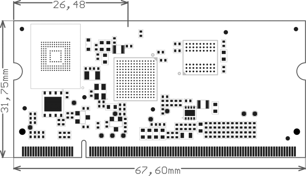
Dimensions
