VisionSOM-G2L Datasheet and Pinout
From SomLabs Wiki

VisionSOM-G2L Datasheet and Pinout
General description
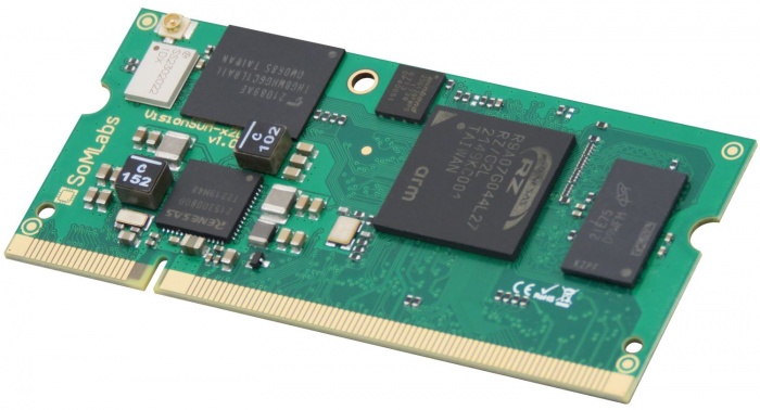
The VisionSOM-G2L family is a SODIMM-sized SoM based on the Renesas dual core RZ/G2L application processor which features third real-time core Cortex-M33. The VisionSOM-G2L family offers energy efficient dual ARM Cortex-A55 cores (at speed up to 1.2GHz) and ARM Cortex-M33 core (at speed up to 200MHz) as well as a 3D Graphics Processing Unit (ARM Mali-G31 GPU @500MHz, 1920x1080 @60fps) with Open GL 3.2ES/OpenCL 2.0 (Full Profile) capabilities and Video Codec Processor (VCP) with 1920x1080 @30fps.
The VisionSOM-G2L is a multimedia and video oriented, highly integrated SoM (System on Module) featuring high computation power, optinally integrated 2.4GHz Wi-Fi and Bluetooth v5.1 connectivity. The option of integrated, fully certified Wi-Fi and Bluetooth module simplifies the carrier board design and is ideally suited for wireless application. The VisionSOM-G2L provides a variety memory configuration, including 1GB of fast and efficient DDR4 and eMMC Flash that meets our customers requirements.
The SoM supports connections to a variety of interfaces: two high-speed USB 2.0 with integrated PHY, dual Ethernet 1Gbit, audio, MIPI-DSI display output with optional touch panel, MIPI-CSI camera input with scaling processor, serial communication interfaces including 2xCAN. In addition, the system supports industrial grade embedded applications.
SoMLabs also provides a complete hardware and software development board for the SoM in the form of a carrier board and optional TFT display and touch panel.
Applications
- IoT Edge Devices
- IoT gateways
- Machine vision equipment
- AI+ML Decision/Recognition Systems
- Robotics
- Human-machine Interfaces (HMI)
- IP Cameras
- Home Appliances
- Home Automation – Smart Home
- Residential gateways
- Industrial embedded Linux computer
- Fitness/outdoor equipment
Features
- Powered by dual core Renesas RZ/G2L application processor (R9A07G044L27GBG)
- Dual ARM Cortex-A55 core at speed up to 1.2GHz
- ARM Cortex-M33 core at speed up to 200MHz
- Integrated 3D GPU (ARM Mali-G31 @500MHz)
- 1GB RAM (DDR4)
- Up to 32GB eMMC memory
- Optional Murata radio module 2.4GHz Wi-Fi and Bluetooth v5.1
- Built-in dual USB 2.0 interface
- Built-in 2xCAN-FD interfaces
- Built-in MIPI-DSI display interface
- Built-in MIPI-CSI camera interface
- Power-efficient and cost-optimized solution
- Ideal for industrial IoT and embedded applications
- Integrated security features
Pictures of SOM versions
| Version | Photo |
|---|---|
| eMMC |
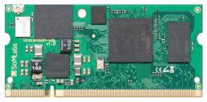 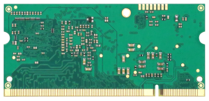 |
| WiFi/BT module is available for all memory configurations. |
Ordering info
| SLS | Product type SLS - System on Module |
| 2 | SOM Name 2 - High Performance VisionSOM SODIM200 module |
| 2 | CPU Family 1 - Renesas RZ/G2L family |
| CpuType | CPU Type RG2LDC - RZ/G2L dual Cortex-A55 + Cortex-M33 + DRP-AI |
| Clock | CPU Clock Speed 1200C - 1.2GHz |
| RamSize | DDR4 RAM Size 01GR - 1GB (1024MB) |
| FlashSize | eMMC Memory Size 04GE - 4GB eMMC 08GE - 8GB eMMC 16GE - 16GB eMMC 32GE - 32GB eMMC |
| SF | Special Features 0SF - No Special Features 1WB - Built-in 2.4GHz Wi-Fi and Bluetooth v5.1 |
| TEMP | Operating Temperature E - Extended: -25 to +70 C I - Industrial: -40 to +85 C |
Block Diagram
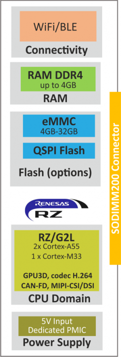
Operating ranges
| Parameter | Value | Unit | Comment |
|---|---|---|---|
| Power Supply | Connected to VDD-5V0 SODIM200 pins | ||
| Max. input GPIO voltage | In 3.3V power domain | ||
| Max. input GPIO voltage | In 1.8V power domain | ||
| Environment temperature1 | oC | Industrial range w/o WiFi module | |
| Industrial range with WiFi module | |||
| Consumer range |
Note:
1. Maximum MPU junction temperature is +105oC.
2. Junction temperature determines MPU lifetime. Details: NXP AN13214 Application Note.
Electrical parameters
| SOM signal name |
Parameter | Value | Unit | ||
|---|---|---|---|---|---|
| Min. | Typ. | Max. | |||
| VDD-5V | Supply Voltage (Input) | 4.0 | 5.0 | 5.5 | V |
| VDD-1V8 | Output power supply for external 1.8V accesories | - | - | 0.31 | A |
| VDD-3V3 | Output power supply for external 3.3V accesories | - | - | 0.32 | A |
| VGPIO @1V8 | GPIO Input Voltage | 0 | - | 2.05 | V |
| VGPIO @3V3 | GPIO Input Voltage | 0 | - | 3.62 | V |
| VUSB0-VBUS | USB VBUS Input Voltage | 0 | - | 5.253 | V |
| VETH0 | I/O voltage for Ethernet 0 | 0 | - | 1.8 | V |
| VETH1 | I/O voltage for Ethernet 1 | 0 | - | 1.8 or 3.34 | V |
| VJTAG | I/O voltage for Ethernet 1 | 0 | - | 1.85 | V |
| VADC-IN | Input voltage for ADC-CHx6 | 0 | - | 1.8 | V |
Notes:
1. Total current on both VDD-1V8 outputs.
1. Total current on both VDD-3V3 outputs.
3. Input current is limited by 2,8kOhm resistor connected in series.
4. Depends on logic state on ET1-VDD-SEL (ET1-VDD-SEL='0' -> V=1.8V, ET1-VDD-SEL='1' or left open -> V=3.3V, internally pull-up'ed.).
5. JTAG/SWD interface lines are 1.8V compatible.
6. "x" means 0...7.
SoM pinout
Important notes:
1. Detail pin configurations description you can find, edit and arrange in dedicated SCFG file (with free "Smart Configurator" tool).
2. On-board eMMC memory is connected to SDIO0 interface.
3. Optional on-board QSPI Flash memory is connected to QSPI0 interface.
4. SDIO1 interface is used to communication with Murata 1DX radio module.
5. UART2 is used to communication with BT-BLE interatted with Murata 1DX radio module.
6. I2C3 is used to communication with on-board PMIC.
| SOM pin numer | Default function | GPIO | BGA456 ball | Notes |
|---|---|---|---|---|
| 1 | GND | Power | - | |
| 2 | GND | Power | - | |
| 3 | ET0-PHY-RST | P47-1 | A20 | 1.8V Power Domain GPIO mode not allowed |
| 4 | PWR-GOOD | Output | PMIC power-good signalling for external devices | |
| 5 | ET0-INT | P47-0 | B20 | 3.3V Power Domain |
| 6 | PWR-ON | Input | PMIC PWRON input (on-off function) Internal pull-down Connect to GND if not used Connect to VDD-3V3 with external pull-up resistor (4.7kOhm) and pushbutton to GND if used | |
| 7 | ET0-MDIO | I/O | U1 | 1.8V Power Domain GPIO mode not allowed |
| 8 | PWR-FAIL | Input | PMIC enable-input: PWR-FAIL='0' -> SOM power supply is off PWR-FAIL='1' or left open -> SOM power supply is on Can bue used as cold-reset input (active low) | |
| 9 | ET0-MDC | I/O | U2 | 1.8V Power Domain GPIO mode not allowed |
| 10 | RESET-OUT | Output | RESET output for external peripherals | |
| 11 | GND | Power | - | |
| 12 | RESET-IN | Input | MPU reset input, active low | |
| 13 | ET0-RXC | I/O | P2 | 1.8V Power Domain GPIO mode not allowed |
| 14 | GND | Power | - | |
| 15 | ET0-RX-CTL | I/O | P1 | 1.8V Power Domain GPIO mode not allowed |
| 16 | UART0-RXD | P38-1 | B15 | 3.3V Power Domain |
| 17 | ET0-RXD0 | I/O | R2 | 1.8V Power Domain GPIO mode not allowed |
| 18 | UART0-TXD | P38-0 | A15 | 3.3V Power Domain |
| 19 | ET0-RXD1 | I/O | R1 | 1.8V Power Domain GPIO mode not allowed |
| 20 | UART1-CTS | P41-0 | E17 | 3.3V Power Domain |
| 21 | ET0-RXD2 | I/O | T2 | 1.8V Power Domain GPIO mode not allowed |
| 22 | UART1-RTS | P41-1 | A18 | 3.3V Power Domain |
| 23 | ET0-RXD3 | I/O | T1 | 1.8V Power Domain GPIO mode not allowed |
| 24 | UART1-RXD | P40-0 | C17 | 3.3V Power Domain |
| 25 | GND | Power | - | |
| 26 | UART1-TXD | P40-1 | B17 | 3.3V Power Domain |
| 27 | ET0-TX-CTL | I/O | N2 | 1.8V Power Domain GPIO mode not allowed |
| 28 | UART4-RXD | P2-1 | A13 | 3.3V Power Domain |
| 29 | ET0-TXC | I/O | N1 | 1.8V Power Domain GPIO mode not allowed |
| 30 | UART4-TXD | P2-0 | B13 | 3.3V Power Domain |
| 31 | ET0-TXD3 | I/O | N1 | 1.8V Power Domain GPIO mode not allowed |
| 32 | UART3-RXD | P0-1 | B12 | 3.3V Power Domain |
| 33 | ET0-TXD2 | I/O | L2 | 1.8V Power Domain GPIO mode not allowed |
| 34 | UART3-TXD | P0-0 | A11 | 3.3V Power Domain |
| 35 | ET0-TXD1 | I/O | M2 | 1.8V Power Domain GPIO mode not allowed |
| 36 | VBAT-RTC | Power | - | RTC 3V battery |
| 37 | ET0-TXD0 | I/O | M1 | 1.8V Power Domain GPIO mode not allowed |
| 38 | GND | Power | - | |
| 39 | VDD-1V8 | Power | 1.8V output for external devices, max. 300 mA | |
| 40 | VDD-1V8 | Power | 1.8V output for external devices, max. 300 mA | |
| 41 | VDD-5V0 | Power | External power supply | |
| 42 | VDD-5V0 | Power | External power supply | |
| 43 | VDD-5V0 | Power | External power supply | |
| 44 | VDD-5V0 | Power | External power supply | |
| 45 | VDD-5V0 | Power | External power supply | |
| 46 | VDD-5V0 | Power | External power supply | |
| 47 | VDD-5V0 | Power | External power supply | |
| 48 | VDD-5V0 | Power | External power supply | |
| 49 | VDD-5V0 | Power | External power supply | |
| 50 | VDD-5V0 | Power | External power supply | |
| 51 | NC | Not Connected | - | |
| 52 | NC | Not Connected | - | |
| 53 | VDD-3V3 | Power | 3.3V output for external devices, max. 300mA | |
| 54 | VDD-3V3 | Power | - | 3.3V output for external devices, max. 300mA |
| 55 | GND | Power | - | |
| 56 | SYSLED | P42-0 | AG4 | 3.3V Power Domain |
| 57 | VPROG | NC | - | For SoMLabs purposes only, leave unconnected |
| 58 | GND | Power | - | |
| 59 | BOOT-RECOVERY | Input | BOOT input, active low during reset | |
| 61 | GND | Power | - | |
| 62 | SSI0-RXD | P7-1 | AH28 | 3.3V Power Domain |
| 63 | ET1-VDD-SEL | Input | Ethernet 1 (ET1) interface voltage selection: ET1-VDD-SEL='0' -> V=1.8V ET1-VDD-SEL='1' or left open -> V=3.3V The line has internal pull-up. | |
| 64 | SSI0-TXD | P7-0 | AJ28 | 3.3V Power Domain |
| 65 | ET1-PHY-RST | P47-3 | B21 | 3.3V Power Domain |
| 66 | SSI0-RCK | P6-1 | AH27 | 3.3V Power Domain |
| 67 | ET1-INT | P47-2 | A21 | 3.3V Power Domain |
| 68 | SSI0-BCK | P6-0 | AJ27 | 3.3V Power Domain |
| 69 | ET1-MDIO | P37-1 | W1 | 1.8V or 3.3V Power Domain selected by ET1-VDD-SEL GPIO allowed only for 3.3V. |
| 70 | GND | Power | - | |
| 71 | ET1-MDC | P37-0 | W2 | 1.8V or 3.3V Power Domain selected by ET1-VDD-SEL GPIO allowed only for 3.3V. |
| 72 | CAN1-RX | P13-0 | AF23 | 3.3V Power Domain |
| 73 | GND | Power | - | |
| 74 | CAN1-TX | P12-1 | AE23 | 3.3V Power Domain |
| 75 | ET1-RXC | P33-1 | AC1 | 1.8V or 3.3V Power Domain selected by ET1-VDD-SEL GPIO allowed only for 3.3V. |
| 76 | CAN0-RX | P42-2 | AJ3 | 3.3V Power Domain |
| 77 | ET1-RX-CTL | P34-0 | AC2 | 1.8V or 3.3V Power Domain selected by ET1-VDD-SEL GPIO allowed only for 3.3V. |
| 78 | CAN0-TX | P42-1 | AE7 | 3.3V Power Domain |
| 79 | ET1-RXD0 | P34-1 | AC3 | 1.8V or 3.3V Power Domain selected by ET1-VDD-SEL GPIO allowed only for 3.3V. |
| 80 | GND | Power | - | |
| 81 | ET1-RXD1 | P35-0 | AC4 | 1.8V or 3.3V Power Domain selected by ET1-VDD-SEL GPIO allowed only for 3.3V. |
| 82 | I2C3-SCL-EXT | P46-3 | D13 | I2C interface used for on-board PMIC configuration Built-in pull-up resistor 2.2kOhm connected to 3.3V 3.3V Power Domain |
| 83 | ET1-RXD2 | P35-1 | AB4 | 1.8V or 3.3V Power Domain selected by ET1-VDD-SEL GPIO allowed only for 3.3V. |
| 84 | I2C3-SDA-EXT | P46-2 | C12 | I2C interface used for on-board PMIC configuration Built-in pull-up resistor 2.2kOhm connected to 3.3V 3.3V Power Domain |
| 85 | ET1-RXD3 | P36-0 | AB3 | 1.8V or 3.3V Power Domain selected by ET1-VDD-SEL GPIO allowed only for 3.3V. |
| 86 | I2C2-SCL | P42-4 | AC5 | Built-in pull-up resistor 2.2kOhm connected to 3.3V |
| 87 | GND | Power | - | |
| 88 | I2C2-SDA | P42-3 | AH3 | Built-in pull-up resistor 2.2kOhm connected to 3.3V |
| 89 | ET1-TX-CTL | P29-1 | Y1 | 1.8V or 3.3V Power Domain selected by ET1-VDD-SEL GPIO allowed only for 3.3V. |
| 90 | P19-0 | P19-0 | B1 | 3.3V Power Domain |
| 91 | ET1-TXC | P29-0 | AB2 | 1.8V or 3.3V Power Domain selected by ET1-VDD-SEL GPIO allowed only for 3.3V. |
| 92 | P18-0 | P18-0 | C2 | 3.3V Power Domain |
| 93 | ET1-TXD3 | P31-1 | Y2 | 1.8V or 3.3V Power Domain selected by ET1-VDD-SEL GPIO allowed only for 3.3V. |
| 94 | GND | Power | - | |
| 95 | ET1-TXD2 | P31-0 | AA1 | 1.8V or 3.3V Power Domain selected by ET1-VDD-SEL GPIO allowed only for 3.3V. |
| 96 | P18-1 | P18-1 | D3 | 3.3V Power Domain |
| 97 | ET1-TXD1 | P30-1 | AA2 | 1.8V or 3.3V Power Domain selected by ET1-VDD-SEL GPIO allowed only for 3.3V. |
| 98 | P45-0 | P45-0 | A8 | 3.3V Power Domain |
| 99 | ET1-TXD0 | P30-0 | AB1 | 1.8V or 3.3V Power Domain selected by ET1-VDD-SEL GPIO allowed only for 3.3V. |
| 100 | P45-2 | P45-2 | A9 | 3.3V Power Domain |
| 101 | GND | Power | - | |
| 102 | P45-3 | P45-3 | B9 | 3.3V Power Domain |
| 103 | USB1-D_N | Analog I/O | - | |
| 104 | P46-0 | P46-0 | B10 | 3.3V Power Domain |
| 105 | USB1-D_P | Analog I/O | - | |
| 106 | P46-1 | P46-1 | A10 | 3.3V Power Domain |
| 107 | USB1-OC | P8-1 | AJ20 | 3.3V Power Domain |
| 108 | P45-1 | P45-1 | D12 | 3.3V Power Domain |
| 109 | USB1-EN | P8-0 | AH19 | 3.3V Power Domain |
| 110 | P1-1 | P1-1 | A12 | 3.3V Power Domain |
| 111 | GND | Power | - | |
| 112 | P3-1 | P3-1 | B14 | 3.3V Power Domain |
| 113 | USB0-OC | P5-0 | AJ4 | 3.3V Power Domain |
| 114 | P1-0 | P1-0 | C13 | 3.3V Power Domain |
| 115 | USB0-EN | P4-0 | AJ5 | 3.3V Power Domain |
| 116 | GND | Power | - | |
| 117 | USB0-ID | P5-1 | AH4 | 3.3V Power Domain |
| 118 | P3-0 | P3-0 | A14 | 3.3V Power Domain |
| 119 | USB0-D_N | Analog I/O | - | |
| 120 | P48-2 | P48-2 | A22 | 3.3V Power Domain |
| 121 | USB0-D_P | Analog I/O | - | |
| 122 | P4-1 | P4-1 | AH6 | 3.3V Power Domain |
| 123 | USB0-VBUS | Dedicated input | AH10 | 3.3V Power Domain |
| 124 | P7-2 | P7-2 | AJ19 | 3.3V Power Domain |
| 125 | GND | Power | - | |
| 126 | GND | Power | - | |
| 127 | P11-1 | P11-1 | AF22 | 3.3V Power Domain |
| 128 | P11-0 | P11-0 | AG22 | 3.3V Power Domain |
| 129 | P8-2 | P8-2 | AH20 | 3.3V Power Domain |
| 130 | P12-0 | P12-0 | AE22 | 3.3V Power Domain |
| 131 | P9-1 | P9-1 | AH21 | 3.3V Power Domain |
| 132 | P13-1 | P13-1 | AG23 | 3.3V Power Domain |
| 133 | P9-0 | P9-0 | AJ21 | 3.3V Power Domain |
| 134 | SPI1-SSL | P44-3 | B19 | 3.3V Power Domain |
| 135 | SPI0-SSL | P43-3 | B19 | 3.3V Power Domain |
| 136 | SPI1-MISO | P44-2 | D18 | 3.3V Power Domain |
| 137 | SPI0-MISO | P43-2 | E18 | 3.3V Power Domain |
| 138 | SPI1-MOSI | P44-1 | F17 | 3.3V Power Domain |
| 139 | SPI0-MOSI | P43-1 | D17 | 3.3V Power Domain |
| 140 | SPI1-CLK | P44-0 | A19 | 3.3V Power Domain |
| 141 | SPI0-CLK | P43-0 | B18 | 3.3V Power Domain |
| 142 | GND | Power | - | |
| 143 | GND | Power | - | |
| 144 | I2C1-SCL | Dedicated I2C line | C23 | RIIC1_SCL Built-in pull-up resistor 2.2kOhm connected to 3.3V |
| 145 | P14-0 | P14-0 | AF27 | 3.3V Power Domain |
| 146 | I2C1-SDA | Dedicated I2C line | A24 | RIIC1_SDA Built-in pull-up resistor 2.2kOhm connected to 3.3V |
| 147 | P10-1 | P10-1 | AH22 | 3.3V Power Domain |
| 148 | I2C0-SCL | Dedicated I2C line | B24 | RIIC0_SCL Built-in pull-up resistor 2.2kOhm connected to 3.3V |
| 149 | P10-0 | P10-0 | AJ22 | 3.3V Power Domain |
| 150 | I2C0-SDA | Dedicated I2C line | A25 | RIIC0_SDA Built-in pull-up resistor 2.2kOhm connected to 3.3V |
| 151 | P15-0 | P15-0 | AH23 | 3.3V Power Domain |
| 152 | GND | Power | - | |
| 153 | P14-1 | P14-1 | AJ23 | 3.3V Power Domain |
| 154 | ADC-CH7 | Dedicated analog input | 12-bit ADC, max. 1.8V on input | |
| 155 | P16-0 | P16-0 | AH24 | 3.3V Power Domain |
| 156 | ADC-CH6 | Dedicated analog input | 12-bit ADC, max. 1.8V on input | |
| 157 | P15-1 | P15-1 | AJ24 | 3.3V Power Domain |
| 158 | ADC-CH5 | Dedicated analog input | 12-bit ADC, max. 1.8V on input | |
| 159 | P17-0 | P17-0 | AH25 | 3.3V Power Domain |
| 160 | ADC-CH4 | Dedicated analog input | 12-bit ADC, max. 1.8V on input | |
| 160 | SSI-MCLK | AUDIO-CLK | E12 | Reference clock output (for audio codec) |
| 161 | P16-1 | P16-1 | AJ25 | 3.3V Power Domain |
| 162 | ADC-CH3 | Dedicated analog input | 12-bit ADC, max. 1.8V on input | |
| 163 | P17-2 | P17-2 | AH26 | 3.3V Power Domain |
| 164 | ADC-CH2 | Dedicated analog input | 12-bit ADC, max. 1.8V on input | |
| 165 | P17-1 | P17-1 | AJ26 | 3.3V Power Domain |
| 166 | ADC-CH1 | Dedicated analog input | 12-bit ADC, max. 1.8V on input | |
| 167 | P13-2 | P13-2 | AG26 | 3.3V Power Domain |
| 168 | ADC-CH0 | Dedicated analog input | 12-bit ADC, max. 1.8V on input | |
| 169 | GND | Power | - | |
| 170 | GND | Power | - | |
| 171 | DSI-DATA3_P | Analog I/O | AH18 | MIPI-DSI line |
| 172 | CSI-DATA3_N | Analog I/O | AH11 | MIPI-CSI line |
| 173 | DSI-DATA3_N | Analog I/O | AJ18 | MIPI-DSI line |
| 174 | CSI-DATA3_P | Analog I/O | AJ11 | MIPI-CSI line |
| 175 | GND | Power | - | |
| 176 | GND | Power | - | |
| 177 | DSI-DATA2_P | Analog I/O | AH15 | MIPI-DSI line |
| 178 | CSI-DATA2_N | Analog I/O | AH14 | MIPI-CSI line |
| 179 | DSI-DATA2_N | Analog I/O | AJ15 | MIPI-DSI line |
| 180 | CSI-DATA2_P | Analog I/O | AJ14 | MIPI-CSI line |
| 181 | GND | Power | - | |
| 182 | GND | Power | - | |
| 183 | DSI-CLK_P | Analog I/O | AG17 | MIPI-DSI line |
| 184 | CSI-CLK_N | Analog I/O | AG12 | MIPI-CSI line |
| 185 | DSI-CLK_N | Analog I/O | AG18 | MIPI-DSI line |
| 186 | CSI-CLK_P | Analog I/O | AG13 | MIPI-CSI line |
| 187 | GND | Power | - | |
| 188 | GND | Power | - | |
| 189 | DSI-DATA1_P | Analog I/O | AH17 | MIPI-DSI line |
| 190 | CSI-DATA1_N | Analog I/O | AH12 | MIPI-CSI line |
| 191 | DSI-DATA1_N | Analog I/O | AJ17 | MIPI-DSI line |
| 192 | CSI-DATA1_P | Analog I/O | AJ12 | MIPI-CSI line |
| 193 | GND | Power | - | |
| 194 | GND | Power | - | |
| 195 | DSI-DATA0_P | Analog I/O | AH16 | MIPI-DSI line |
| 196 | CSI-DATA0_N | Analog I/O | AH13 | MIPI-CSI line |
| 197 | DSI-DATA0_N | Analog I/O | AJ16 | MIPI-DSI line |
| 198 | CSI-DATA0_P | Analog I/O | AJ13 | MIPI-CSI line |
| 199 | GND | Power | - | |
| 200 | GND | Power | - | |
| - | WLAN-ENABLE | P40-2 | A17 | 1DX radio module line (WiFi) Not available externally |
| - | WLAN-H-WAKE | P19-1 | B2 | 1DX radio module line (WiFi) Not available externally |
| - | SD1-CLK | - | H3 | 1DX radio module line (WiFi) Not available externally |
| - | SD1-CMD | - | J2 | 1DX radio module line (WiFi) Not available externally |
| - | SD1-DATA0 | - | H1 | 1DX radio module line (WiFi) Not available externally |
| - | SD1-DATA1 | - | H2 | 1DX radio module line (WiFi) Not available externally |
| - | SD1-DATA2 | - | K2 | 1DX radio module line (WiFi) Not available externally |
| - | SD1-DATA3 | - | J1 | 1DX radio module line (WiFi) Not available externally |
| - | UART2-RXD | P48-1 | B23 | 1DX radio module line (BLE) Not available externally |
| - | UART2-TXD | P48-0 | B22 | 1DX radio module line (BLE) Not available externally |
| - | UART2-RTS | P48-4 | B23 | 1DX radio module line (BLE) Not available externally |
| - | UART2-CTS | P48-3 | C22 | 1DX radio module line (BLE) Not available externally |
| - | BT-DEV-WAKE | P39-0 | A16 | 1DX radio module line (BLE) Not available externally |
| - | BT-HOST-WAKE | P39-1 | C15 | 1DX radio module line (BLE) Not available externally |
| - | BT-REG-ON | P39-3 | B16 | 1DX radio module line (BLE) Not available externally |
| - | JTAG-TMS | AD2 | JTAG interface 1.8V Power Domain | |
| - | JTAG-TCK | AE1 | JTAG interface 1.8V Power Domain | |
| - | JTAG-TDO | AE2 | JTAG interface 1.8V Power Domain | |
| - | JTAG-TDI | AF1 | JTAG interface 1.8V Power Domain | |
| - | JTAG-TRST | AF2 | JTAG interface 1.8V Power Domain | |
| - | QSPI-CLK | C4 | Optional on-board QSPI Flash (W25Q128FWPIG) | |
| - | QSPI-IO0 | A3 | Optional on-board QSPI Flash (W25Q128FWPIG) | |
| - | QSPI-IO1 | B3 | Optional on-board QSPI Flash (W25Q128FWPIG) | |
| - | QSPI-IO2 | A4 | Optional on-board QSPI Flash (W25Q128FWPIG) | |
| - | QSPI-IO3 | B4 | Optional on-board QSPI Flash (W25Q128FWPIG) | |
| - | QSPI-SS | A2 | Optional on-board QSPI Flash (W25Q128FWPIG) | |
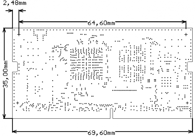
Dimensions
