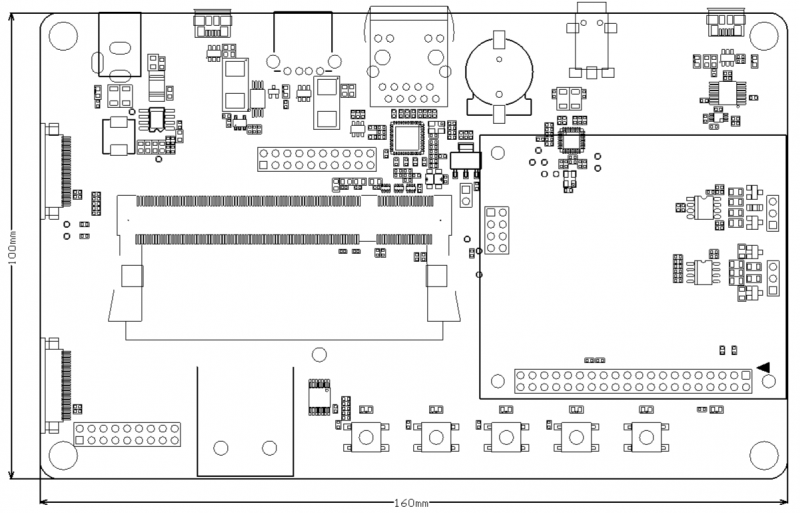
VisionCB-x2L-STD Datasheet and Pinout
From SomLabs Wiki

VisionCB-x2L-STD v.1.2 Datasheet and Pinout
General description
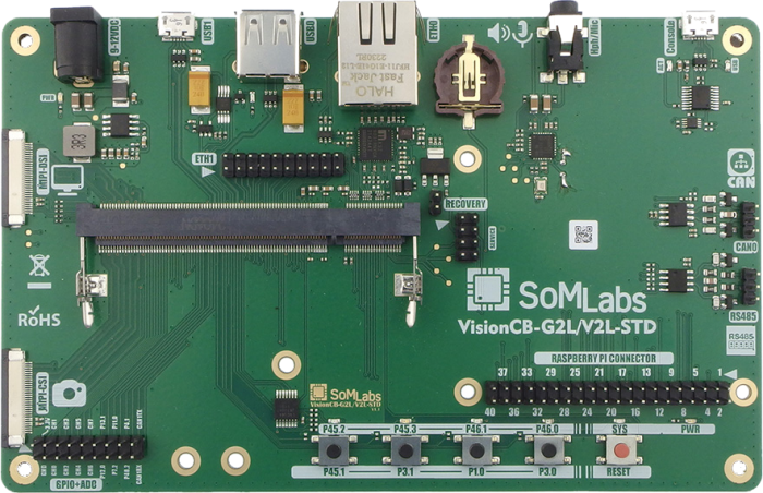
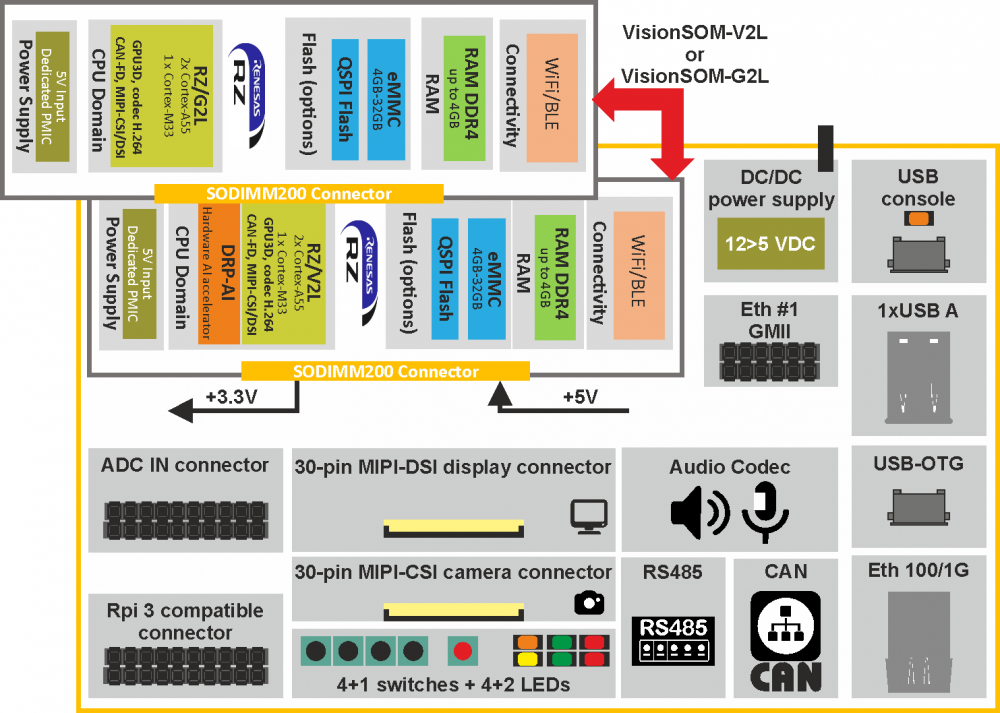
The VisionCB-x2L-STD (with SOM equipped with Renesas RZ/V2L and RZ/G2L MPUs compatible) is a carrier board for the VisionSOM-V2L and VisionSOM-G2L family of computer-on-modules which are powered by dual-core Renesas MPUs (2 x ARM Cortex-A55 + Cortex-M33). The carrier board, together with a System on Module (SoM), makes a complete development platform similar to SBC. The carrier board houses the most common interfaces such as USB, Ethernet, CAN, RS485, audio codec, etc. A large variety of interfaces allows to use it as both a complete development platform or as a stand-alone end-product. The VisionCB-x2L-STD is equipped with a simple user interface consisting of 4 buttons and 4 LEDs. VisionCB-x2L-STD carrier board is also equipped with a large number of popular peripherals, including: RS485, CAN, 10/100/1G Ethernet, MIPI display and camera connectors, serial console port on USB vCOM.
Applications
- Multimedia
- Video streaming
- Image inspection
- VisionAI gateway
- Doorbell systems
- EV chargers
- Smart agriculture gateways
- Industrial embedded Linux computer
- Home Appliances
- Home Automation – Smart Home
- Human-machine Interfaces (HMI)
- Point-of-sales (POS) terminals
- IoT gateways
- Machine vision equipment
- Robotics
- Fitness/outdoor equipment
Features
- Carrier Board compatible with the VisionSOM-G2L and VisionSOM-V2L families of modules based on dual core, heterogenous Renesas RZ/V2L and RZ/G2L application processors
- SoM Connector: SODIMM200
- Expansion Connectors:
- ADC+GPIO connector 2x9 Pin Header (Male)
- Raspberry Pi Compatible Connectors 2x20 Pin Header (Male)
- Ethernet #1 (GMII) Connector Pin Header (Male)
- Communication Connectors:
- 1x Ethernet 10/100/1000Mbit/s (RJ45)
- 1x CAN (1x3 Pin Header, Male)
- 1x RS-485 (1x3 Pin Header, Male)
- 1x USB Host Type A connectors
- 1x USB OTG Micro AB connector
- 1x Console MicroUSB B connector
- Audio Interface:
- Mini-jack 3.5mm (headphones + microphone)
- Display Interface:
- 30-pin FFC/FPC MIPI-DSI (up to 4 lanes)
- Camera Interface:
- 30-pin FFC/FPC MIPI-CSI2 (up to 4 lanes)
- User Interface:
- 4+1 Pushbuttons
- 4+2 LEDs
- External Power Supply 9-12V DC
- Temperature Range: 0 to +70°C
- Board Size: 160mm x 100mm x 21mm
Pictures of VisionCB-x2L-STD v1.2 board
| Version | Photo |
|---|---|
| VisionCB-x2L-STD v1.2 board only |
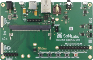 |
| VisionCB-x2L-STD v1.2 with VisionSOM-x2L |
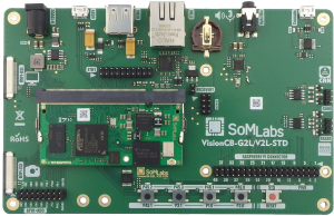 |
Ordering info
Block Diagram
Electrical parameters
| Parameter | Value | Units | Comment | ||
|---|---|---|---|---|---|
| Min. | Typ. | Max. | |||
| Power Supply | 9.0 | 12.0 | 15.0 | V | Positive pole on central connector of J200 |
| Supply current | - | - | 0.13 | A | Excluding LCD, USB and antoher external loads |
| LCD/Camera Power Supply (logic) |
3.25 | 3.3 | 3.35 | V | - |
| LCD/Camera Power Supply (backlight and aux) |
4.75 | 4.87 | 4.95 | V | - |
| Arduino GPIO voltage | 3.3 | V | - | ||
Power supply connector
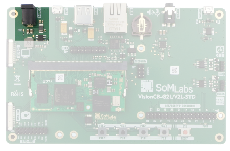
The VisionCB-x2L-STD is equipped with external power source connector with pin diameter 2.5mm and hole diameter 6mm. The voltage of the external power source should be within the range 9-12 VDC.
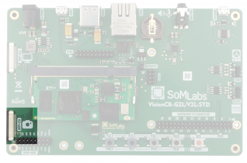
Camera MIPI-CSI interface (FPC/FFC30, 0.5mm)
| Pin | MPU signal | Signal | Description | |
|---|---|---|---|---|
| 1 | GND | - | - | |
| 2 | CSI-CLK-P | - | - | |
| 3 | CSI-CLK-P | - | - | |
| 4 | GND | - | - | |
| 5 | CSI-DATA0-P | - | - | |
| 6 | CSI-DATA0-N | - | - | |
| 7 | GND | - | - | |
| 8 | CSI-DATA1-P | - | - | |
| 9 | CSI-DATA1-N | - | - | |
| 10 | GND | - | - | - |
| 11 | CSI-DATA2-P | - | - | |
| 12 | CSI-DATA2-N | - | - | |
| 13 | GND | - | - | |
| 14 | CSI-DATA3-P | - | - | |
| 15 | CSI-DATA3-N | - | - | |
| 16 | GND | - | - | |
| 17 | I2C1-SCL | RIIC1_SCL | Camera confguration I2C interface (3.3V), pull-uped with 2.2k | |
| 18 | I2C1-SDA | RIIC1_SDA | Camera confguration I2C interface (3.3V), pull-uped with 2.2k | |
| 19 | GND | - | - | |
| 20 | SAI3-TXFS | xx | Optional audio interface | |
| 21 | SAI3-TXC | xx | Optional audio interface | |
| 22 | - | - | - | |
| 23 | GND | - | - | |
| 24 | +3.3V | - | Power supply for external devices | |
| 25 | +3.3V | - | Power supply for external devices | |
| 26 | +5V | - | Power supply for external devices | |
| 27 | +5V | - | Power supply for external devices | |
| 28 | - | - | - | |
| 29 | - | - | - | |
| 30 | GND | - | - |
Note:
1. The first pin of the MIPI-CSI connector is located in its upper part.
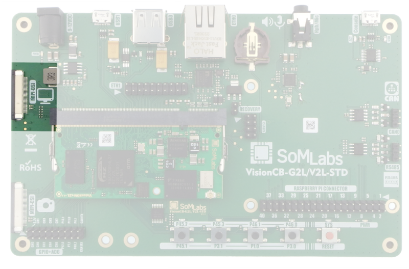
Display MIPI-DSI interface (FPC/FFC30, 0.5mm)
| Pin | Signal | MPU signal | Description |
|---|---|---|---|
| 1 | GND | - | |
| 2 | DSI-CLK-P | - | - |
| 3 | DSI-CLK-P | - | - |
| 4 | GND | - | - |
| 5 | DSI-DATA0-P | - | - |
| 6 | DSI-DATA0-N | - | - |
| 7 | GND | - | - |
| 8 | DSI-DATA1-P | - | - |
| 9 | DSI-DATA1-N | - | - |
| 10 | GND | - | - |
| 11 | DSI-DATA2-P | - | - |
| 12 | DSI-DATA2-N | - | - |
| 13 | GND | - | - |
| 14 | DSI-DATA3-P | - | - |
| 15 | DSI-DATA3-N | - | - |
| 16 | GND | - | - |
| 17 | I2C1-SCL | RIIC1_SCL | Display confguration I2C interface (3.3V), pull-uped with 2.2k |
| 18 | I2C1-SDA | RIIC1_SDA | Display confguration I2C interface (3.3V), pull-uped with 2.2k |
| 19 | GND | - | - |
| 20 | DISP-RST | P13-2 | Optional display reset signal |
| 21 | TP-INT | P17-1 | Optional touch-panel interrupt signal |
| 22 | TP-RST | P17-2 | Optional touch-panel reset signal |
| 23 | GND | - | - |
| 24 | +3.3V | Power supply for external devices | |
| 25 | +3.3V | Power supply for external devices | |
| 26 | +5V | Power supply for external devices | |
| 27 | +5V | Power supply for external devices | |
| 28 | DSI-BL-PWM | P16-0 | Optional PWM backlight signal |
| 29 | DSI-BL-EN | P16-1 | Optional ENABLE backlight signal |
| 30 | GND | - | - |
Note:
1. The first pin of the MIPI-DSI connector is located in its upper part.
USB Console Port and Segger J-Link debugger
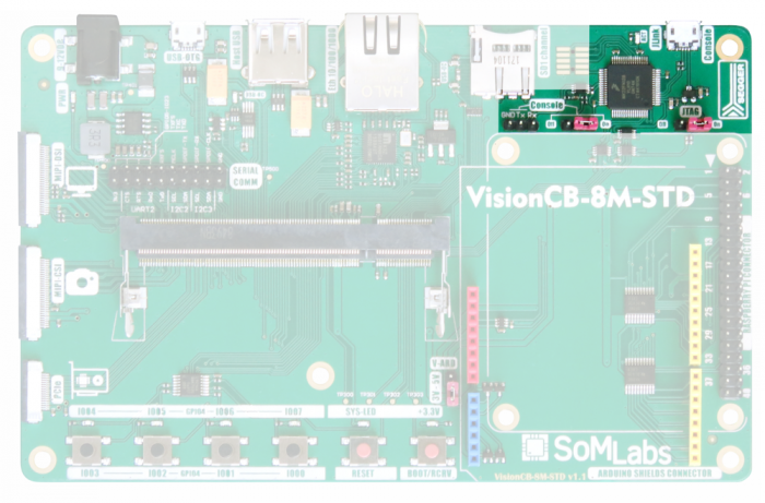
| MPU Port | GPIO | Description |
|---|---|---|
| CONSOLE-TXD | UART4-TXD | Signal connected to J304 pin 2 |
| CONSOLE-RXD | UART4-RXD | Signal connected to J304 pin 3 |
Notes:
1. Linux console port (UART4 in MPU) uses vCOM interface provided by built-in debugger Segger J-Link.
2. vCOM can be disconnected from MPU with JP801 (jumper CONSOLE in position ON or OFF).
3. Lines TXD and RXD of UART4 are easy to monitoring thanks to using J304 gold-pins.
4. Debug JTAG interface can be disconnected from MPU with JP800 (jumper JTAG in position ON or OFF).
MicroSD card interface (J308)
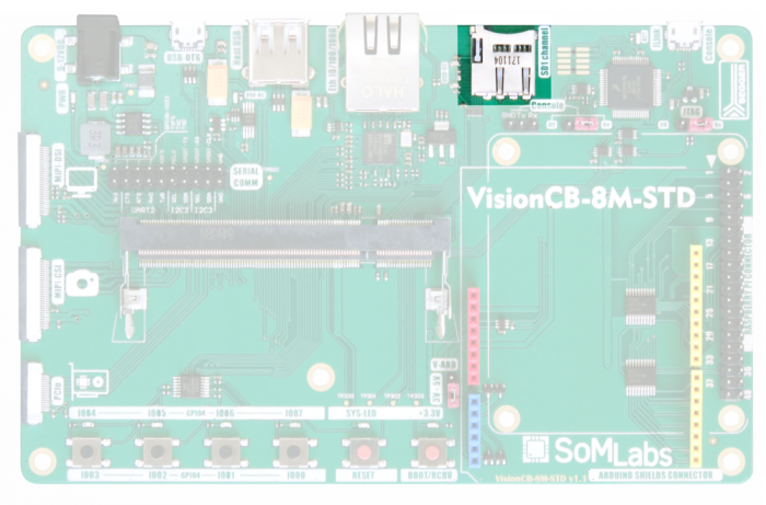
| Connector pin | SD card signal | SOM pin |
|---|---|---|
| 1 | DATA2 | SD1-DATA2 |
| 2 | DATA3 | SD1-DATA3 |
| 3 | CMD | SD1-CMD |
| 4 | NVCC-SDIO | Voltage selected 1.8/3.3V by SD1 driver |
| 5 | CLK | SD1-CLK |
| 6 | GND | - |
| 7 | DATA0 | SD1-DATA0 |
| 8 | DATA1 | SD1-DATA1 |
| 9 | CARD-DETECT | SD1-CD |
Raspberry Pi compatible I/O header
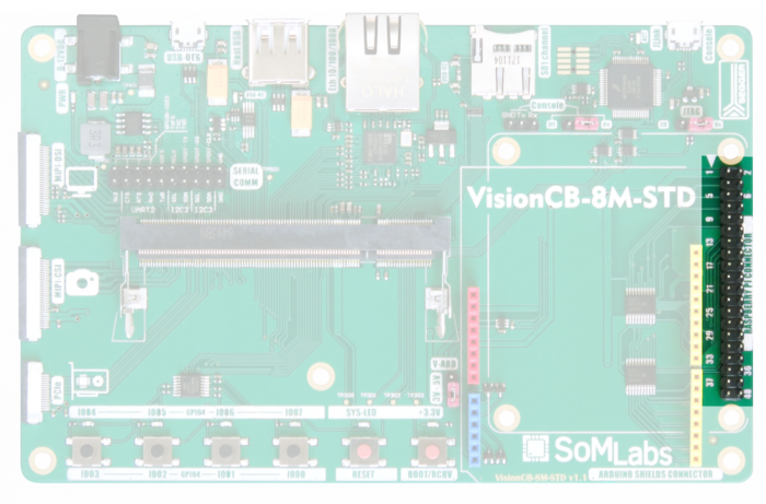
| Pin | Default function name | Description |
|---|---|---|
| 1 | +3.3V | +3.3V generated by DC/DC built-in SOM (limited current load) |
| 2 | +5V | +5V generated by carrier board built-in DC/DC converter |
| 3 | I2C1-SDA | I2C1-SDA line |
| 4 | +5V | +5V generated by carrier board built-in DC/DC converter |
| 5 | I2C1-SDA | I2C1-SDA line |
| 6 | GND | - |
| 7 | GPIO4-IO09 | Universal GPIO with 3.3V logic levels |
| 8 | UART3-TXD | Default: UART3 TXD line or universal GPIO with 3.3V logic levels |
| 9 | GND | - |
| 10 | UART3-RXD | Default: UART3 RXD line or universal GPIO with 3.3V logic levels |
| 11 | GPIO4-IO08 | Universal GPIO with 3.3V logic levels |
| 12 | SPI2-CLK | Default: SPI2-CLK line or universal GPIO with 3.3V logic levels |
| 13 | - | - |
| 14 | GND | - |
| 15 | - | - |
| 16 | SPI2-MISO | Default: SPI2-MISO line or universal GPIO with 3.3V logic levels |
| 17 | +3.3V | +3.3V generated by DC/DC built-in SOM (limited current load) |
| 18 | SPI2-MOSI | Default: SPI2-MOSI line or universal GPIO with 3.3V logic levels |
| 19 | SPI1-MOSI | Default: SPI1-MOSI line or universal GPIO with 3.3V logic levels |
| 20 | GND | - |
| 21 | SPI1-MISO | Default: SPI1-MISO line or universal GPIO with 3.3V logic levels |
| 22 | SPI2-SS0 | Default: SPI2-SS0 line or universal GPIO with 3.3V logic levels |
| 23 | SPI1-CLK | Default: SPI1-CLK line or universal GPIO with 3.3V logic levels |
| 24 | SPI1-SS0 | Default: SPI1-SS0 line or universal GPIO with 3.3V logic levels |
| 25 | GND | - |
| 26 | GPIO-IO22 | Universal GPIO with 3.3V logic levels |
| 27 | - | - |
| 28 | - | - |
| 29 | GPIO4-IO12 | Universal GPIO with 3.3V logic levels |
| 30 | GND | - |
| 31 | GPIO4-IO13 | Universal GPIO with 3.3V logic levels |
| 32 | GPIO4-IO20 | Universal GPIO with 3.3V logic levels |
| 33 | GPIO4-IO14 | Universal GPIO with 3.3V logic levels |
| 34 | GND | - |
| 35 | GPIO4-IO14 | Universal GPIO with 3.3V logic levels |
| 36 | GPIO4-IO19 | Universal GPIO with 3.3V logic levels |
| 37 | GPIO4-IO16 | Universal GPIO with 3.3V logic levels |
| 38 | GPIO4-IO18 | Universal GPIO with 3.3V logic levels |
| 39 | GND | - |
| 40 | GPIO4-IO17 | Universal GPIO with 3.3V logic levels |
Arduino Uno compatible I/O header
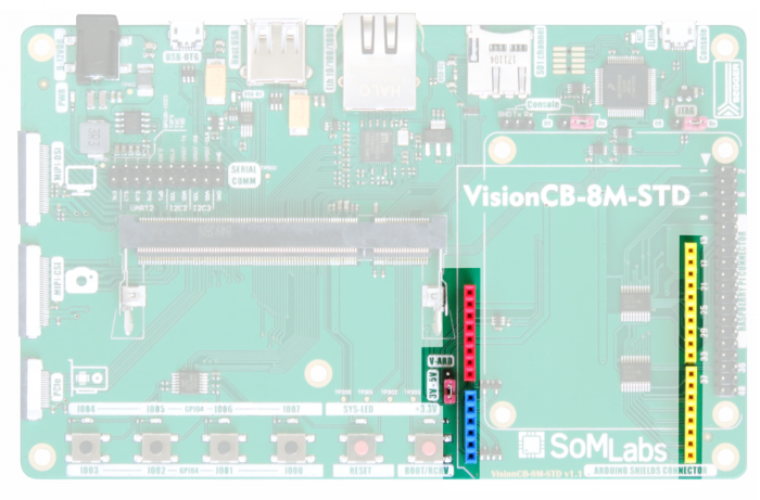
| Pin | Arduino name | Default function name | Description |
|---|---|---|---|
| Power connector J700, red connector | |||
| 1 | - | - | - |
| 2 | IOREF | VDD-ARDUINO-IO | Selected +3.3V or +5V (with V-ARD jumper). |
| 3 | RESET | POR-B | External reset input, active L. |
| 4 | 3.3V | VCC-3V3 | +3.3V generated by internal SOM LDO converter (limited load current). |
| 5 | 5V | VCC-5V0 | +5V generated by carrier board built-in DC/DC converter. |
| 6 | GND | GND | - |
| 7 | GND | GND | - |
| 8 | VIN | VCC-3V3 | +3.3V generated by internal SOM LDO converter (limited load current). |
| Analog inputs connector J702, blue connector | |||
| 1 | AIN0 | - | Not internally connected. |
| 2 | AIN1 | - | Not internally connected. |
| 3 | AIN2 | - | Not internally connected. |
| 4 | AIN3 | - | Not internally connected. |
| 5 | - | - | Not internally connected. |
| 6 | - | - | Not internally connected. |
| Digital I/Os connector J704, yellow connector | |||
| 1 | DIO0 | UART3-RXD | Default: UART3-RXD line or universal GPIO with 3.3/5V logic levels. |
| 2 | DIO1 | UART3-TXD | Default: UART3-TXD line or universal GPIO with 3.3/5V logic levels. |
| 3 | DIO2 | GPIO4-IO15 | Universal GPIO with 3.3/5V logic levels. |
| 4 | DIO3 | GPIO4-IO14 | Universal GPIO with 3.3/5V logic levels. |
| 5 | DIO4 | GPIO4-IO13 | Universal GPIO with 3.3/5V logic levels. |
| 6 | DIO5 | GPIO4-IO12 | Universal GPIO with 3.3/5V logic levels. |
| 7 | DIO6 | GPIO4-IO11 | Universal GPIO with 3.3/5V logic levels. |
| 8 | DIO7 | GPIO4-IO10 | Universal GPIO with 3.3/5V logic levels. |
| Digital I/Os connector J703, yellow connector | |||
| 1 | DIO8 | GPIO4-IO08 | Universal GPIO with 3.3/5V logic levels. |
| 2 | DIO9 | GPIO4-IO09 | Universal GPIO with 3.3/5V logic levels. |
| 3 | DIO10 | SPI1-SS0 | Default: SPI1-SS0 line or universal GPIO with 3.3/5V logic levels. |
| 4 | DIO11 | SPI1-MOSI | Default: SPI1-MOSI line or universal GPIO with 3.3/5V logic levels. |
| 5 | DIO12 | SPI1-MISO | Default: SPI1-MISO line or universal GPIO with 3.3/5V logic levels. |
| 6 | DIO13 | SPI1-CLK | Default: SPI1-CLK line or universal GPIO with 3.3/5V logic levels. |
| 7 | GND | GND | - |
| 8 | AREF | VDD-ARDUINO-IO | +3.3V or +5V selected with V-ARD jumper. |
| 9 | DIO14 | I2C1-SCL | Default: I2C1-SCL line or universal GPIO with 3.3/5V logic levels. |
| 10 | DIO15 | I2C1-SDA | Default: I2C1-SDA line or universal GPIO with 3.3/5V logic levels. |
Notes:
1. I/O logic levels are selected 3.3/5V with V-ARD jumper.
2. RESET line is 3.3 and 5V compatible.
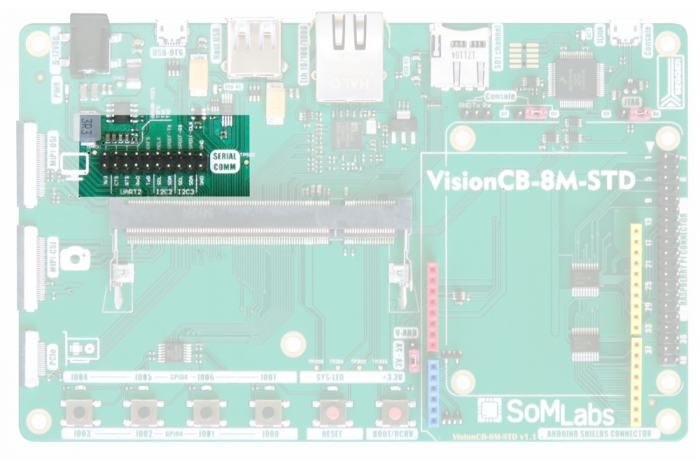
Serial Communication/GPIO header (J305)
| Pin | Default function name | Description |
|---|---|---|
| 1 | +3.3V | +3.3V generated by DC/DC built-in SOM (limited current load) |
| 2 | GPIO5-IO23 | Universal GPIO with 3.3V logic levels By default is connected to MIPI-DSI (J301) as touch-panel interrupt line (with 47k pull-up) |
| 3 | UART2-CTS | By default: UART2-CTS or universal GPIO with 3.3V logic levels |
| 4 | SAI3-TXFS | By default: SAI3-TXFS or universal GPIO with 3.3V logic levels Connected to MIPI-CSI (J302) |
| 5 | UART2-RTS | By default: UART2-RTS or universal GPIO with 3.3V logic levels |
| 6 | SAI3-TXC | By default: SAI3-TXC or universal GPIO with 3.3V logic levels Connected to MIPI-CSI (J302) |
| 7 | UART2-RXD | By default: UART2-RXD or universal GPIO with 3.3V logic levels |
| 8 | SAI3-TXD | By default: SAI3-TXD or universal GPIO with 3.3V logic levels |
| 9 | UART2-TXD | By default: UART2-TXD or universal GPIO with 3.3V logic levels |
| 10 | SAI3-RXFS | By default: SAI3-RXFS or universal GPIO with 3.3V logic levels By default is connected to MIPI-DSI (J301) as display module reset signal |
| 11 | I2C2-SCL | By default: I2C2-SCL or universal GPIO with 3.3V logic levels Default I2C port for PCIe (J303), MIPI-DSI (J301) and MIPI-CSI (J302) |
| 12 | SAI3-MCLK | By default: SAI3-MCLK or universal GPIO with 3.3V logic levels |
| 13 | I2C2-SDA | By default: I2C2-SDA or universal GPIO with 3.3V logic levels Default I2C port for PCIe (J303), MIPI-DSI (J301) and MIPI-CSI (J302) |
| 14 | SPDIF-TX | By default: SPDIC-TX or universal GPIO with 3.3V logic levels By default is connected to MIPI-DSI (J301) as touch-panel reset signal |
| 15 | I2C3-SCL | By default: I2C3-SCL or universal GPIO with 3.3V logic levels |
| 16 | SPDIF-RX | By default: I2C3-SCL or universal GPIO with 3.3V logic levels By default is connected to MIPI-DSI (J301) as display module PWM backlight control |
| 17 | I2C3-SDA | By default: I2C3-SDA or universal GPIO with 3.3V logic levels |
| 18 | SPDIF-CLK | By default: SPDIF-CLK or universal GPIO with 3.3V logic levels By default is connected to MIPI-DSI (J301) as display module on/off signal |
| 19 | GND | - |
| 20 | GND | - |
User Interface (switches and LEDs)
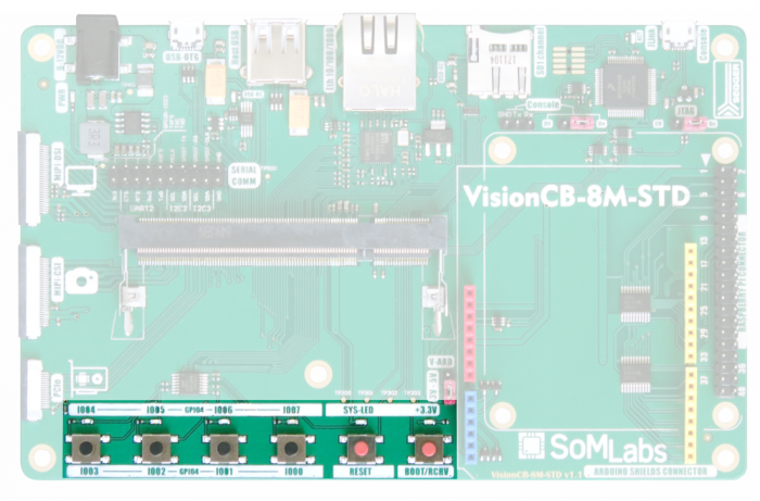
User switches
| Switch | GPIO | Description |
|---|---|---|
| S305 (black, most on the left) | GPIO4-IO03 | 47k pull-up |
| S304 | GPIO4-IO02 | 47k pull-up |
| S303 | GPIO4-IO01 | 47k pull-up |
| S302 (black, most on the right) | GPIO4-IO00 | 47k pull-up |
System switches
| Switch | Signal name | Description |
|---|---|---|
| S301 (left, red) | Reset | - |
| S300 (right, red) | BOOT-RECOVERY | - |
User LEDs
| LED | GPIO | Description |
|---|---|---|
| D303 (most on the left) | GPIO4-IO04 | User LED1, buffered with inverter |
| D302 | GPIO4-IO05 | User LED2, buffered with inverter |
| D301 | GPIO4-IO06 | User LED3, buffered with inverter |
| D300 (most on the right) | GPIO4-IO07 | User LED4, buffered with inverter |
System LEDs
| LED | GPIO | Description |
|---|---|---|
| D304 | SYS-LED | System function monitoring |
| D305 | - | Power LED (3.3V) |
Dimensions
