VisionSOM-RT117x Datasheet and Pinout
From SomLabs Wiki

VisionSOM-RT117x Datasheet and Pinout
General description

Thex VisionSOM-RT117x family is a SODIMM-sized SoM based on the NXP i.MX RT1170 family real-time microcontroller which features an advanced implementation of a dual ARM Cortex-M7 and Cortex-M4 cores. The Cortex-M7 operates at up to 1 GHz and the Cortex-M4 up to 400 MHz with 2 MB on-chip RAM. The real-time microcontroller (MCU) family offers various memory interfaces and a wide range of connectivity interfaces including 3x Ethernet up to Gbps with TSN/AVB, UART, SPI, I2C, USB and 3x CAN-FD. The i.MX RT1170 provides advanced embedded security including secure boot and crypto engines.
The VisionSOM-RT117x is a low power highly integrated SoM (System-on-Module) featuring high computation performance, real-time functionality and MCU usability. High security enabled by AES-128/256 and RSA4096, HAB and On-the-fly QSPI Flash Decryption together with 2D graphical acceleration make an ideally suited solution for home and industrial control systems, wireless application, communication solutions and real-time systems.
The system supports industrial grade targeting embedded application.
SOMLabs also provides a complete hardware and software development board for the SoM in the form of a carrier board and optional TFT display with MIPI-DSI and touch panel.
Applications
- Industrial embedded RTOS computer
- Home Appliances
- Air Conditioning
- Building Security
- Fleet Management
- Heat Metering
- Home Automation – Smart Home
- Human-machine Interfaces (HMI)
- Motor Drives
- Cash Register
- Intermediate Flight Controller
- Smart grid Infrastructure
- IoT gateways
- Residential getaways
- Smart Lock
- Robotics
- Toys and Board Games
Features
- Powered by NXP i.MX RT117x application processor
- Single (Cortex-M7) or dual (Cortex-M7 + Cortex-M4) core solution
- Core clock up to 1GHz (single core, commercial grade MCU)
- 2MB on-chip RAM memory
- up to 128MB SDRAM memory
- up to 32MB QuadSPI Flash memory
- Power-efficient and cost-optimized solution
- Ideal for industrial IoT and embedded applications
- FreeRTOS support
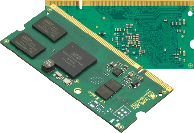
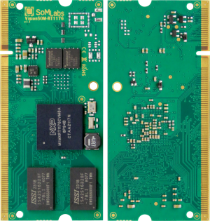
Pictures of SOM versions
| Version | Photo |
|---|---|
| SDRAM & dual QSPI |
 |
Ordering info
| SLS | Product type SLS - System on Module |
| 1 | SOM Name 1 - VisionSOM SODIMM200 |
| 4 | CPU Family 4 - i.MX RT117x |
| CpuType | CPU Type RT1176 - i.MX RT 1176 |
| Clock | CPU Clock Speed 800C - 800MHz |
| RamSize | RAM Size 0R - No RAM 32R - 32MB 64R - 64MB 128R - 128MB |
| FlashSize | Flash Size Type and Density 4QSPI - 4MB QSPI Flash 16QSPI - 16MB QSPI Flash 32QSPI - 32MB QSPI Flash 64OF - 64MB Octal Flash |
| SF | Special Features 0SF - No Special Features |
| TEMP | Operating Temperature C - Consumer: 0 to +70 C I - Industrial: -40 to +85 C |
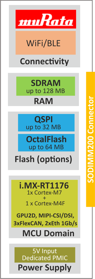
Block Diagram

Operating ranges
| Parameter | Value | Unit | Comment |
|---|---|---|---|
| External Power Supply | Connected to VDD-5V0 SODIMM pins | ||
| Internal DC-DC converter output voltage | Connected to VDD-3V3 SODIMM pins | ||
| Internal DC-DC converter output current | Maximum value for external loads | ||
| Input GPIO_DISP_B1 domain voltage | - | ||
| Input NVCC_SNVS domain voltage | NVCC_SNVS is internally powered from VDD_SNVS_ANA = 1.75V1 | ||
| Input IO domains voltage | Maximum value Regarding domains: - NVCC_SD1 - NVCC_LPSR - NVCC_DISP2 - NVCC_GPIO - NVCC_SD1 | ||
| Input VBUS (USB1 and USB2) voltage | - | ||
| Environment temperature2 | oC | Industrial range | |
| Consumer range |
Note:
1. All system control lines (i.a. ONOFF, POR_B, PMIC_STBY_REQ, PMIC_ON_REQ) are powered from NVCC_SNVS domain, connected to VDD_SNVS_ANA=1.75V.
2. Maximum MPU junction temperature is +105oC (industrial version) or +95oC (consumer version).
Electrical parameters
| SOM signal name |
Parameter | Value | Units | ||
|---|---|---|---|---|---|
| Min. | Typ. | Max. | |||
| VDD-5V | Supply Voltage | 4.5 | 5.0 | 5.5 | V |
| - | Total Supply Current1 | - | TBD | TBD | mA |
| GPIOs in GPIO_DISP_B1 domain | Input Voltage | 0 | 1.8 | 1.982 | V |
| GPIOs in NVCC_SNVS domain | Input Voltage | 0 | 1.75 | 1.852 | V |
| GPIOs in NVCC_SD1, NVCC_LPSR, NVCC_DISP2, NVCC_GPIO, NVCC_SD1 domains | Input Voltage | 0 | 3.3 | 3.962 | V |
| USB Vbus | USB Supply | 0 | 5 | 5.62 | V |
| System Control Lines | - | 0 | 1.75 | 1.852, 3 | V |
| VDD-3V3 | Internal DC/DC converter Output Voltage |
3.15 | 3.3 | 3.35 | V |
| - | Internal DC/DC converter Output Current |
- | - | 0.2 | A |
| VDD-COIN-3V | SNVS Backup Battery Supply |
2.82 | - | 3.6 | V |
Notes:
1. Excluding external load connected to VDD-3V3 lines.
2. Applying the maximum voltage higer than recommended results in shorten lifetime.
3. All system control lines (i.a. ONOFF, POR_B, PMIC_STBY_REQ, PMIC_ON_REQ) are powered from NVCC_SNVS domain, supplied from internal MCU LDO output (VDD_SNVS_ANA=1.75V).
Pinout
Important notes:
1. Detail pin configurations description you can find, edit and arrange in dedicated MEX files (with free "i.MX Pin Tool" configurational tool):
VisionSOM-RT117x with QSPI Flash and SDRAM memory on board
| SOM pin number | Default function | GPIO | Ball number | Notes |
|---|---|---|---|---|
| 1 | GND | - | - | - |
| 2 | GND | - | - | - |
| 3 | JTAG.TMS | GPIO_LPSR_15 | U7 | 3.3V power domain |
| 4 | WAKEUP | T8 | 1.75V VDD_SNVS_ANA power domain A GPIO powered by SNVS domain power supply which can be configured as wakeup source in SNVS mode | |
| 5 | JTAG.TCK | GPIO_LPSR_14 | T6 | 3.3V power domain |
| 6 | ON-OFF | - | U10 | 1.75V VDD_SNVS_ANA power domain A brief connection to GND in the OFF mode causes the internal power management state machine to change the state to ON. In the ON mode, a brief connection to GND generates an interrupt (intended to be a software-controllable power-down). Approximately five seconds (or more) to GND causes a forced OFF. Both boot mode inputs can be disconnected. |
| 7 | JTAG.TDO | GPIO_LPSR_11 | T5 | 3.3V power domain |
| 8 | PMIC-STBY-REQ | - | T9 | 1.75V VDD_SNVS_ANA power domain Internally used |
| 9 | JTAG.TDI | GPIO_LPSR_12 | U5 | 3.3V power domain |
| 10 | RESET | - | T10 | POR-B of MCU line (resets all of the chip except the Secure Non-Volatile Storage (SNVS) block), active low 1.75V VDD_SNVS_ANA power domain |
| 11 | JTAG.TRST | GPIO_LPSR_10 | R5 | 3.3V power domain |
| 12 | RESET-IN | - | - | Active low global reset line (hard reset by turning off the power) |
| 13 | JTAG.MOD | GPIO_LPSR_13 | U6 | 3.3V power domain Line with internal pull-down by 10 kOhm resistor |
| 14 | GND | - | - | - |
| 15 | SD1.DATA1 | GPIO_SD_B1_03 | B17 | WIFI data line or GPIO Available to the user as GPIO only in modules without 1DX radio modules 3.3V power domain |
| 16 | UART2.RXD | GPIO_DISP_B2_11 | A6 | 3.3V power domain |
| 17 | SD1.DATA0 | GPIO_SD_B1_02 | C15 | WIFI data line or GPIO Available to the user as GPIO only in modules without 1DX radio modules 3.3V power domain |
| 18 | UART2.TXD | GPIO_DISP_B2_10 | D9 | 3.3V power domain |
| 19 | GND | - | - | - |
| 20 | UART10.CTS | GPIO_AD_34 | J16 | 3.3V power domain |
| 21 | SD1.CLK | GPIO_SD_B1_01 | D15 | WIFI data line or GPIO Available to the user as GPIO only in modules without 1DX radio modules 3.3V power domain |
| 22 | UART10.RTS | GPIO_AD_35 | G17 | 3.3V power domain |
| 23 | SD1.CMD | GPIO_SD_B1_00 | B16 | WIFI data line or GPIO Available to the user as GPIO only in modules without 1DX radio modules 3.3V power domain |
| 24 | UART10.RXD | GPIO_AD_16 | N17 | 3.3V power domain |
| 25 | SD1.DATA3 | GPIO_SD_B1_05 | A16 | WIFI data line or GPIO Available to the user as GPIO only in modules without 1DX radio modules 3.3V power domain |
| 26 | UART10.TXD | GPIO_AD_15 | M14 | 3.3V power domain |
| 27 | SD1.DATA2 | GPIO_SD_B1_04 | B15 | WIFI data line or GPIO Available to the user as GPIO only in modules without 1DX radio modules 3.3V power domain |
| 28 | UART3.RXD | GPIO_AD_31 | J17 | 3.3V power domain |
| 29 | UART1-EXT.CTS | GPIO_AD_26 | L14 | BT serial interface line or GPIO Available to the user as GPIO only in modules without 1DX radio modules 3.3V power domain |
| 30 | UART3.TXD | GPIO_AD_30 | K17 | 3.3V power domain |
| 31 | UART1-EXT.RTS | GPIO_AD_27 | N16 | BT serial interface line or GPIO Available to the user as GPIO only in modules without 1DX radio modules 3.3V power domain |
| 32 | UART5.RXD | GPIO_AD_29 | M17 | 3.3V power domain |
| 33 | UART1-EXT.RXD | GPIO_AD_25 | M15 | BT serial interface line or GPIO Available to the user as GPIO only in modules without 1DX radio modules 3.3V power domain |
| 34 | UART5.TXD | GPIO_AD_28 | L17 | 3.3V power domain |
| 35 | UART1-EXT.TXD | GPIO_AD_24 | L13 | BT serial interface line or GPIO Available to the user as GPIO only in modules without 1DX radio modules 3.3V power domain |
| 36 | VDD-COIN-3V | - | - | The backup power supply for VDD-SNVS-3V3 domain |
| 37 | GND | - | - | - |
| 38 | GND | - | - | - |
| 39 | VOUT-1V8 | Internally generated by MPU 1.8V for internal peripherals (maximum external load is very limted, details in Electrical Characteristics section of "i.MX RT1170 Crossover Processors Data Sheet for Industrial Products" by NXP) | ||
| 40 | VOUT-1V8 | Internally generated by MPU 1.8V for internal peripherals (maximum external load is very limted, details in Electrical Characteristics section of "i.MX RT1170 Crossover Processors Data Sheet for Industrial Products" by NXP) | ||
| 41 | VDD-5V | Power supply input | ||
| 42 | VDD-5V | Power supply input | ||
| 43 | VDD-5V | Power supply input | ||
| 44 | VDD-5V | Power supply input | ||
| 45 | VDD-5V | Power supply input | ||
| 46 | VDD-5V | Power supply input | ||
| 47 | VDD-5V | Power supply input | ||
| 48 | VDD-5V | Power supply input | ||
| 49 | VDD-5V | Power supply input | ||
| 50 | VDD-5V | Power supply input | ||
| 51 | NC | - | - | - |
| 52 | NC | - | - | - |
| 53 | VOUT-3V3 | Internally generated by PMIC 3.3V for external devices | ||
| 54 | VOUT-3V3 | Internally generated by PMIC 3.3V for external devices | ||
| 55 | GND | - | - | - |
| 56 | DAC-OUT | DAC-OUT | H16 | 12-bit DAC voltage output (range 0-1.8V) |
| 57 | RECOVERY | BOOT-MODE0 | P6 | Boot mode selector, if: RECOVERY = 0 then BOOT-MODE0 = 1, as a result serial loader starts RECOVERY = 1 or open then BOOT-MODE0 = 0, as a result MCU boots from fuses |
| 58 | GND | - | - | - |
| 59 | GND | - | - | - |
| 60 | SAI1.MCLK | GPIO_DISP_B2_03 | D7 | 3.3V power domain |
| 61 | NC | - | - | - |
| 62 | SAI1.RX | GPIO_DISP_B2_06 | C6 | 3.3V power domain |
| 63 | USB1.D_N | USB1 interface analog I/O | ||
| 64 | SAI1.TX | GPIO_DISP_B2_07 | D6 | 3.3V power domain |
| 65 | USB1.D_P | USB1 interface analog I/O | ||
| 66 | SAI1.FSYNC | GPIO_DISP_B2_04 | C7 | 3.3V power domain |
| 67 | USB1.VBUS | - | D17 | USB1 analog domain, input voltage 2.4-5.5V |
| 68 | SAI1.BCLK | GPIO_DISP_B2_05 | C9 | 3.3V power domain |
| 69 | USB1.OC | GPIO_AD_11 | P16 | 3.3V power domain |
| 70 | GND | - | - | - |
| 71 | USB1.EN | GPIO_AD_10 | R17 | 3.3V power domain |
| 72 | CAN2.RX | GPIO_AD_01 | R14 | 3.3V power domain |
| 73 | USB1.ID | GPIO_AD_09 | R16 | 3.3V power domain |
| 74 | CAN2.TX | GPIO_AD_00 | N12 | 3.3V power domain |
| 75 | GND | - | - | - |
| 76 | CAN1.RX | GPIO_AD_07 | T17 | 3.3V power domain |
| 77 | USB2.ID | GPIO_AD_08 | R15 | 3.3V power domain |
| 78 | CAN1.TX | GPIO_AD_06 | N13 | 3.3V power domain |
| 79 | USB2.EN | GPIO_AD_12 | P17 | 3.3V power domain |
| 80 | GND | - | - | - |
| 81 | USB2.OC | GPIO_AD_13 | L12 | 3.3V power domain |
| 82 | I2C2.SCL | GPIO_AD_18 | M16 | 3.3V power domain |
| 83 | USB2.VBUS | - | D16 | USB2 analog domain, input voltage 2.4-5.5V |
| 84 | I2C2.SDA | GPIO_AD_19 | L16 | 3.3V power domain |
| 85 | USB2.D_N | USB2 interface analog I/O | ||
| 86 | I2C1.SCL | GPIO_AD_32 | K16 | 3.3V power domain |
| 87 | USB2.D_P | USB2 interface analog I/O | ||
| 88 | I2C1.SDA | GPIO_AD_33 | H17 | 3.3V power domain |
| 89 | GND | - | - | - |
| 90 | GND | - | - | - |
| 91 | NC | - | - | - |
| 92 | UART8.RTS | GPIO_AD_05 | P13 | 3.3V power domain |
| 93 | NC | - | - | - |
| 94 | UART8.CTS | GPIO_AD_04 | M13 | 3.3V power domain |
| 95 | ENET-QOS.RESET | GPIO_EMC_B1_41 | L1 | 3.3V power domain |
| 96 | UART8.RXD | GPIO_AD_03 | P15 | 3.3V power domain |
| 97 | ENET-QOS.INT | GPIO_EMC_B1_40 | K1 | 3.3V power domain |
| 98 | UART8.TXD | GPIO_AD_02 | R13 | 3.3V power domain |
| 99 | ENET-QOS.MDIO | GPIO_EMC_B2_20 | R3 | 3.3V power domain |
| 100 | GPIO3-13 | GPIO_AD_14 | N14 | 3.3V power domain |
| 101 | ENET-QOS.MDC | GPIO_EMC_B2_19 | U2 | 3.3V power domain |
| 102 | GPIO3-21 | GPIO_AD_22 | K12 | 3.3V power domain |
| 103 | GND | - | - | - |
| 104 | GPIO3-22 | GPIO_AD_23 | J12 | 3.3V power domain |
| 105 | ENET-QOS.RXC | GPIO_DISP_B1_01 | D13 | 1.8V power domain |
| 106 | GPIO5-03 | GPIO_DISP_B2_02 | E9 | 3.3V power domain |
| 107 | ENET-QOS.RX-CTL | GPIO_DISP_B1_00 | E13 | 1.8V power domain |
| 108 | GPIO5-10 | GPIO_DISP_B2_09 | D8 | 3.3V power domain |
| 109 | ENET-QOS.RXD0 | GPIO_DISP_B1_02 | D11 | 1.8V power domain |
| 110 | GPIO5-01 | GPIO_DISP_B2_00 | E8 | 3.3V power domain |
| 111 | ENET-QOS.RXD1 | GPIO_DISP_B1_03 | E11 | 1.8V power domain |
| 112 | GPIO5-02 | GPIO_DISP_B2_01 | F8 | 3.3V power domain |
| 113 | ENET-QOS.RXD2 | GPIO_DISP_B1_04 | E10 | 1.8V power domain |
| 114 | GPIO5-09 | GPIO_DISP_B2_08 | B5 | 3.3V power domain |
| 115 | ENET-QOS.RXD3 | GPIO_DISP_B1_05 | C11 | 1.8V power domain |
| 116 | GND | - | - | - |
| 117 | GND | - | - | - |
| 118 | SPI4.CS0 | GPIO_DISP_B2_15 | A4 | 3.3V power domain |
| 119 | ENET-QOS.TX-CTL | GPIO_DISP_B1_10 | B14 | 1.8V power domain |
| 120 | SPI4.IN | GPIO_DISP_B2_13 | A5 | 3.3V power domain |
| 121 | ENET-QOS.TXC | GPIO_DISP_B1_11 | A14 | 1.8V power domain |
| 122 | SPI4.OUT | GPIO_DISP_B2_14 | A7 | 3.3V power domain |
| 123 | ENET-QOS.TXD3 | GPIO_DISP_B1_06 | D10 | 1.8V power domain |
| 124 | SPI4.SCK | GPIO_DISP_B2_12 | B6 | 3.3V power domain |
| 125 | ENET-QOS.TXD2 | GPIO_DISP_B1_07 | E12 | 1.8V power domain |
| 126 | GND | - | - | - |
| 127 | ENET-QOS.TXD1 | GPIO_DISP_B1_08 | A15 | 1.8V power domain |
| 128 | GPIO-SVNS.0 | GPIO_SNVS_00 | R10 | 1.75V VDD_SNVS_ANA power domain |
| 129 | ENET-QOS.TXD0 | GPIO_DISP_B1_09 | C13 | 1.8V power domain |
| 130 | GPIO-SVNS.1 | GPIO_SNVS_01 | P10 | 1.75V VDD_SNVS_ANA power domain |
| 131 | GND | - | - | - |
| 132 | GPIO-SVNS.2 | GPIO_SNVS_02 | L9 | 1.75V VDD_SNVS_ANA power domain |
| 133 | NC | - | - | - |
| 134 | GPIO-SVNS.3 | GPIO_SNVS_03 | M10 | 1.75V VDD_SNVS_ANA power domain |
| 135 | NC | - | - | - |
| 136 | GPIO-SVNS.4 | GPIO_SNVS_04 | N10 | 1.75V VDD_SNVS_ANA power domain |
| 137 | NC | - | - | - |
| 138 | GPIO-SVNS.5 | GPIO_SNVS_05 | P9 | 1.75V VDD_SNVS_ANA power domain |
| 139 | UART12.CTS | GPIO_LPSR_05 | N8 | 3.3V power domain |
| 140 | GPIO-SVNS.6 | GPIO_SNVS_06 | M9 | 1.75V VDD_SNVS_ANA power domain |
| 141 | UART12.RTS | GPIO_LPSR_04 | N7 | 3.3V power domain |
| 142 | GPIO-SVNS.7 | GPIO_SNVS_07 | R9 | 1.75V VDD_SNVS_ANA power domain |
| 143 | UART12.RXD | GPIO_LPSR_01 | R6 | 3.3V power domain |
| 144 | GPIO-SVNS.8 | GPIO_SNVS_08 | N9 | 1.75V VDD_SNVS_ANA power domain |
| 145 | UART12.TXD | GPIO_LPSR_00 | N6 | 3.3V power domain |
| 146 | GPIO-SVNS.9 | GPIO_SNVS_09 | R11 | 1.75V VDD_SNVS_ANA power domain |
| 147 | NC | - | - | - |
| 148 | GND | - | - | - |
| 149 | I2C5.SCL | GPIO_LPSR_09 | P5 | 3.3V power domain |
| 150 | I2C6.SCL | GPIO_LPSR_07 | R8 | 3.3V power domain |
| 151 | I2C5.SDA | GPIO_LPSR_08 | U8 | 3.3V power domain |
| 152 | I2C6.SDA | GPIO_LPSR_06 | P8 | 3.3V power domain |
| 153 | GND | - | - | - |
| 154 | NC | - | - | - |
| 155 | NC | - | - | - |
| 156 | NC | - | - | - |
| 157 | NC | - | - | - |
| 158 | NC | - | - | - |
| 159 | NC | - | - | - |
| 160 | NC | - | - | - |
| 161 | NC | - | - | - |
| 162 | NC | - | - | - |
| 163 | NC | - | - | - |
| 164 | NC | - | - | - |
| 165 | NC | - | - | - |
| 166 | NC | - | - | - |
| 167 | NC | - | - | - |
| 168 | NC | - | - | - |
| 169 | GND | - | - | - |
| 170 | GND | - | - | - |
| 171 | NC | - | - | - |
| 172 | NC | - | - | - |
| 173 | NC | - | - | - |
| 174 | NC | - | - | - |
| 175 | GND | - | - | - |
| 176 | GND | - | - | - |
| 177 | NC | - | - | - |
| 178 | NC | - | - | - |
| 179 | NC | - | - | - |
| 180 | NC | - | - | - |
| 181 | GND | - | - | - |
| 182 | GND | - | - | - |
| 183 | DSI.CLK_P | DSI video output channel analog line | ||
| 184 | CSI.CLK_N | CSI video input channel analog line | ||
| 185 | DSI.CLK_N | DSI video output channel analog line | ||
| 186 | CSI.CLK_P | CSI video input channel analog line | ||
| 187 | GND | - | - | - |
| 188 | GND | - | - | - |
| 189 | DSI.DATA1_P | DSI video output channel analog line | ||
| 190 | CSI.DATA1_N | CSI video input channel analog line | ||
| 191 | DSI.DATA1_N | DSI video output channel analog line | ||
| 192 | CSI.DATA1_P | CSI video input channel analog line | ||
| 193 | GND | - | - | - |
| 194 | GND | - | - | - |
| 195 | DSI.DATA0_P | DSI video output channel analog line | ||
| 196 | CSI.DATA0_N | CSI video input channel analog line | ||
| 197 | DSI.DATA0_N | DSI video output channel analog line | ||
| 198 | CSI.DATA0_P | CSI video input channel analog line | ||
| 199 | GND | - | - | - |
| 200 | GND | - | - | - |
| BOOT0 | GPIO_LPSR_02 | P6 | 3.3V power domain Recovery function Connected with BT-EN (BT_REG_ON) line of 1DX radio module | |
| BOOT1 | GPIO_LPSR_03 | T7 | 3.3V power domain Connected with WLAN-EN (WL_REG_ON) line of 1DX radio module | |
| BT-HWAKE | GPIO_AD_20 | K13 | 3.3V power domain By default configured as GPIO3-19 connected to BT_HOST_WAKE of 1DX radio module | |
| BT-DWAKE | GPIO_AD_21 | K14 | 3.3V power domain By default configured as GPIO3-20 connected to BT_DEV_WAKE of 1 DX radio module | |
| WDOG-B | GPIO_EMC_B2_18 | N3 | Internal hardware watchdog line (not available to the user) | |
| WLAN-WAKE | GPIO_AD_17 | N15 | 3.3V power domain By default configured as GPIO3-16 connected to WL_HOST_WAKE pin of 1DX radio module |
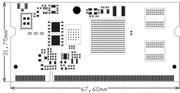
Dimensions
