VisionCB-RT-STD v.1.0 Datasheet and Pinout
From SomLabs Wiki

VisionCB-RT-STD v.1.0 Datasheet and Pinout
General description
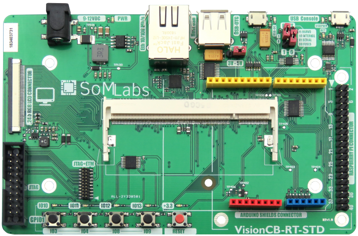
VisionCB-RT-STD is a carrier board for the VisionSOM family of computer-on-modules which are powered by NXP i.MX RT application processors (ARM Cortex-M7). A carrier board, together with a System on Module (SoM), makes a complete development platform similar to SBC. The carrier board houses the most common interfaces such as USB, Ethernet, UART, etc. A large variety of interfaces allows to use it as both a complete development platform or as a stand-alone end-product.
The carrier board connects with the SoM via a standard SODIMM connector.
Applications
- Industrial embedded Linux computer
- Home Appliances
- Home Automation – Smart Home
- Human-machine Interfaces (HMI)
- Point-of-sales (POS) terminals
- Cash Register
- 2D barcode scanners and printers
- Smart grid Infrastructure
- IoT gateways
- Residential getaways
- Machine vision equipment
- Robotics
- Fitness/outdoor equipment
Features
- Carrier Board (Base Board) compatible with the VisionSOM family of modules based on NXP i.MX RT application processors
- SoM connector: SODIMM200
- Expansion Connectors:
- Arduino Uno Rev. 3 1x8, 1x6, 1x8, 1x10 Pin Headers (Female)
- Raspberry Pi compatible connectors 2x20 Pin Header (Male)
- Communication Connectors:
- 1x JTAG connector
- 1x J-Trace connector
- 1x Ethernet 10/100Mbit/s, RJ45
- 1x USB Host Type A connectors
- 1x USB Micro AB connector
- 1x Console MicroUSB B connector (via FTDI FT230 UART to USB converter)
- Display Interface: 50-pin FFC/FPC Parallel RGB – 24-bit, (1366 x 768 Max. Resolution)
- User Interface:
- 5 Pushbuttons
- 5 LEDs
- Boot selector
- Power Supply
- DC connector: Input Voltage 9-12V DC (5.5x2.1 connector)
- MicroUSB connector: Input Voltage 5V DC
- Temperature Range: 0 to +70°C
- Board Size: 145mm x 90mm x 17mm
Pictures of VisionCB-RT-STD v1.0 board
| Version | Photo |
|---|---|
| VisionCB-RT-STD v1.0 board only |
 |
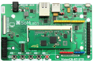
| VisionCB-RT-STD v1.0 board with VisionSOM-RT |
 |
Ordering info
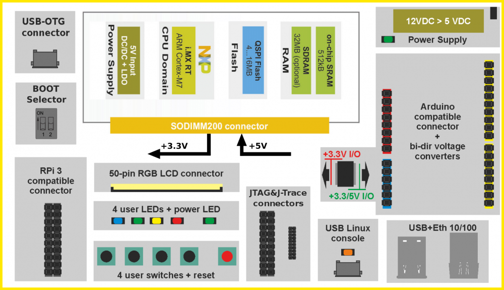
Block Diagram
Electrical parameters
| Parameter | Value | Units | Comment | ||
|---|---|---|---|---|---|
| Min. | Typ. | Max. | |||
| Power Supply (J100 input) | 9.0 | 11.0 | 12.0 | V | Positive pole on central connector of J100 |
| Supply current | - | - | 0.15 | A | Excluding LCD, USB and antoher external loads |
| USB power supply | 4.75 | 4.9 | 5.5 | V | On J201 (Linux USB console connector) |
| Input GPIO voltage (J405) | 0 | - | 3.3 | V | LCD-RGB connector |
| Input GPIO voltage (J504) | 0 | - | 3.3 | V | Raspberry Pi compatible |
| Input GPIO voltage (J502, J503) | 0 | - | 3.3/5 | V | Arduino compatible connector (digital I/O) |
| Input GPIO voltage (J501) | 0 | - | 3.3 | V | Arduino compatible connector (analog inputs) |
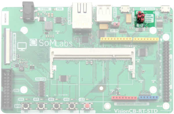
Boot Selector
| BOOTx | Boot Mode | |
|---|---|---|
| BOOT1
GPIO_AD_B0_05 |
BOOT0
GPIO_AD_B0_04 | |
| 1 | 1 | Reserved |
| 1 | 0 | Internal |
| 0 | 1 | Serial |
| 0 | 0 | Fuses |
Note:
1. BOOT0 line is also referred as GPIO-4.
2. By default BOOT0 is pulled down with 10k resistor.
2. By default BOOT1 is pulled up with 1k resistor.
JTAG & JTAG+ETM Connectors
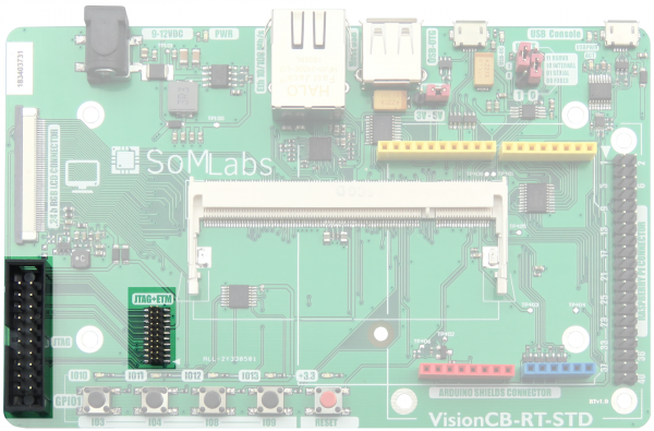
| JTAG Connector | Default function name | MCU pin name |
|---|---|---|
| 1 | VCC-3V3 | NA |
| 2 | - | NA |
| 3 | - | NA |
| 4 | GND | NA |
| 5 | JTAG-TDI | GPIO_AD_B0_09 |
| 6 | GND | NA |
| 7 | JTAG-TMS | GPIO_AD_B0_06 |
| 8 | GND | NA |
| 9 | JTAG-TCK | GPIO_AD_B0_07 |
| 10 | GND | NA |
| 11 | - | NA |
| 12 | GND | NA |
| 13 | JTAG-TDO | GPIO_AD_B0_10 |
| 14 | - | NA |
| 15 | POR-B | POR-B |
| 16 | - | NA |
| 17 | - | NA |
| 18 | - | NA |
| 19 | 5V-Supply (IN) | NA |
| 20 | - | NA |
| JTAG+ETM Connector | Default function name | MCU pin name |
|---|---|---|
| 1 | VCC-3V3 | NA |
| 2 | JTAG-TMS | GPIO_AD_B0_06 |
| 3 | GND | NA |
| 4 | JTAG-TCK | GPIO_AD_B0_07 |
| 5 | GND | NA |
| 6 | JTAG-TDO | GPIO_AD_B0_10 |
| 7 | - | NA |
| 8 | JTAG-TDI | GPIO_AD_B0_09 |
| 9 | - | NA |
| 10 | POR-B | POR-B |
| 11 | 5V-Supply (IN) | NA |
| 12 | LCD-DATA13 | GPIO_B0_12 |
| 13 | 5V-Supply (IN) | NA |
| 14 | LCD-DATA3 | GPIO_B0_04 |
| 15 | GND | NA |
| 16 | LCD-DATA4 | GPIO_B0_05 |
| 17 | GND | NA |
| 18 | LCD-DATA5 | GPIO_B0_06 |
| 19 | GND | NA |
| 20 | LCD-DATA6 | GPIO_B0_07 |
Note:
1. NA - not available.
Raspberry Pi compatible I/O header (J504)
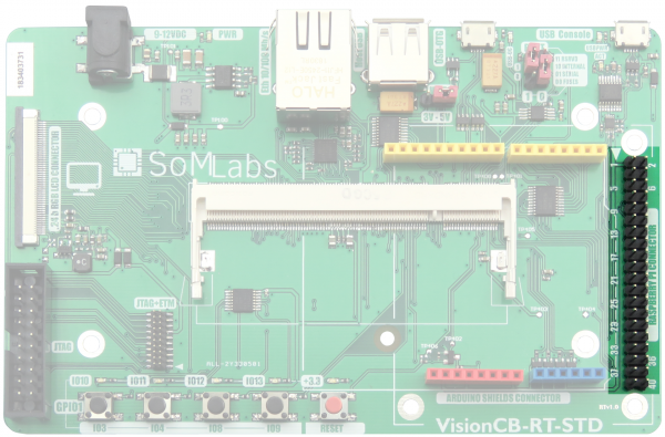
| J504 Pin | Default function name | MCU pin name | Description |
|---|---|---|---|
| 1 | VCC-3V3 | NA | +3.3V generated by internal SOM LDO converter (limited load current). |
| 2 | VCC-5V0 | NA | +5V generated by carrier board built-in DC/DC converter. |
| 3 | UART5-RXD | GPIO_B1_13 | Default: UART5 RxD input or universal GPIO with 3.3V logic levels. |
| 4 | VCC-5V0 | NA | +5V generated by carrier board built-in DC/DC converter. |
| 5 | UART5-TXD | GPIO_B1_12 | Default: UART5 TxD output or universal GPIO with 3.3V logic levels. |
| 6 | GND | NA | - |
| 7 | ENET2-TXD0 | GPIO_B1_15 | Default: ENET2 TXD0 line or universal GPIO with 3.3V logic levels. |
| 8 | UART4-TXD | NC | - |
| 9 | GND | NA | - |
| 10 | UART4-RXD | NC | - |
| 11 | ENET2_CRS_DV | GPIO_AD_B1_15 | Default: ENET2 CRS_DV line or universal GPIO with 3.3V logic levels. |
| 12 | GPIO5 | GPIO_AD_B1_11 | Universal GPIO with 3.3V logic levels. |
| 13 | UART1-CTS | GPIO_AD_B0_14 | Default: UART1 CTS line or universal GPIO with 3.3V logic levels. |
| 14 | GND | NA | - |
| 15 | UART1-RTS | GPIO_AD_B0_15 | Default: UART1 RTS line or universal GPIO with 3.3V logic levels. |
| 16 | GPIO8 | GPIO_AD_B1_09 | Universal GPIO with 3.3V logic levels. |
| 17 | VCC-3V3 | NA | +3.3V generated by internal SOM LDO converter (limited load current) |
| 18 | GPIO9 | GPIO_B1_14 | Universal GPIO with 3.3V logic levels. |
| 19 | UART2-CTS | GPIO_AD_B1_00 | Default: UART2 CTS line or universal GPIO with 3.3V logic levels. |
| 20 | GND | NA | - |
| 21 | UART2-RTS | GPIO_AD_B1_01 | Default: UART2 RTS line or universal GPIO with 3.3V logic levels. |
| 22 | GPIO0 | GPIO_AD_B0_00 | Universal GPIO with 3.3V logic levels. |
| 23 | UART2-RXD | GPIO_AD_B1_03 | Default: UART2 RXD input or universal GPIO with 3.3V logic levels. |
| 24 | UART2-TXD | GPIO_AD_B1_02 | Default: UART2 TXD input or universal GPIO with 3.3V logic levels. |
| 25 | GND | NA | - |
| 26 | ENET2_TXEN | GPIO_AD_B1_12 | Default: ENET2 TXEN line or universal GPIO with 3.3V logic levels. |
| 27 | - | NA | - |
| 28 | - | NA | - |
| 29 | ENET2_TX_CLK | NC | - |
| 30 | GND | NA | - |
| 31 | ENET2_RXER | NC | - |
| 32 | JTAG-MOD | GPIO_AD_B0_08 | Default: JTAG MOD input or universal GPIO with 3.3V logic levels.
Pulled down with 4k7 resistor. |
| 33 | UART3-CTS | GPIO_AD_B1_04 | Default: UART3 CTS line or universal GPIO with 3.3V logic levels. |
| 34 | GND | NA | - |
| 35 | UART3-RTS | GPIO_AD_B1_05 | Default: UART3 RTS line or universal GPIO with 3.3V logic levels. |
| 36 | JTAG-TDO | GPIO_AD_B0_10 | Default: JTAG TDO output or universal GPIO with 3.3V logic levels. |
| 37 | ENET2-RXD1 | NC | - |
| 38 | JTAG-TDI | GPIO_AD_B0_09 | Default: JTAG TDI input or universal GPIO with 3.3V logic levels. |
| 39 | GND | NA | - |
| 40 | JTAG-TMS | GPIO_AD_B0_06 | Default: JTAG TMS output or universal GPIO with 3.3V logic levels. |
Notes:
1. NC - not internally connected.
1. NA - not available.
Arduino compatible I/O headers (J500-J503)
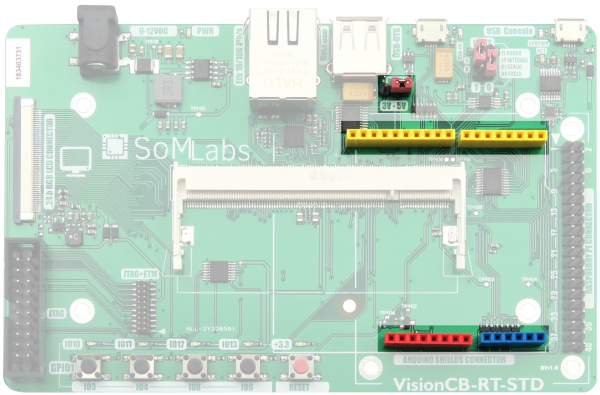
| Pin | Arduino name | Default function name | Description |
|---|---|---|---|
| Power connector J500, red connector | |||
| 1 | - | - | - |
| 2 | IOREF | VCC-3V3 | +3.3V generated by internal SOM LDO converter (limited load current). |
| 3 | RESET | POR-B | External warm reset input, active L. |
| 4 | 3.3V | VCC-3V3 | +3.3V generated by internal SOM LDO converter (limited load current). |
| 5 | 5V | VCC-5V0 | +5V generated by carrier board built-in DC/DC converter. |
| 6 | GND | GND | - |
| 7 | GND | GND | - |
| 8 | VIN | VCC-3V3 | +3.3V generated by internal SOM LDO converter (limited load current). |
| Analog inputs connector J501, blue connector | |||
| 1 | AIN0 | GPIO1 | Universal GPIO with 3.3V logic levels. |
| 2 | AIN1 | GPIO5 | Universal GPIO with 3.3V logic levels. |
| 3 | AIN2 | GPIO8 | Universal GPIO with 3.3V logic levels. |
| 4 | AIN3 | GPIO9 | Universal GPIO with 3.3V logic levels. |
| 5 | - | - | - |
| 6 | - | - | - |
| Digital I/Os connector J503, yellow connector | |||
| 1 | DIO0 | UART4-RXD | Default: UART4 RXD line or universal GPIO with 5V logic levels. |
| 2 | DIO1 | UART4-TXD | Default: UART4 TXD line or universal GPIO with 5V logic levels. |
| 3 | DIO2 | UART3-RTS | Default: UART3 RTS line or universal GPIO with 5V logic levels. |
| 4 | DIO3 | UART3-CTS | Default: UART3 CTS line or universal GPIO with 5V logic levels. |
| 5 | DIO4 | ENET2_RXER | Default: ENET2 RX ER line or universal GPIO with 5V logic levels. |
| 6 | DIO5 | ENET2_TX_CLK | Default: ENET2 TX CLK line or universal GPIO with 5V logic levels. |
| 7 | DIO6 | UART1-RTS | Default: UART1 RTS line or universal GPIO with 5V logic levels. |
| 8 | DIO7 | UART1-CTS | Default: UART1 CTS line or universal GPIO with 5V logic levels. |
| Digital I/Os connector J502, yellow connector | |||
| 1 | DIO8 | ENET2_TXD0 | Default: ENET2 TXD0 line or universal GPIO with 5V logic levels. |
| 2 | DIO9 | ENET2_CRS_DV | Default: ENET2 CRS DV line or universal GPIO with 5V logic levels. |
| 3 | DIO10 | UART2-TXD | Default: UART2 TXD line or universal GPIO with 5V logic levels. |
| 4 | DIO11 | UART2-CTS | Default: UART2 CTS line or universal GPIO with 5V logic levels. |
| 5 | DIO12 | UART2-RTS | Default: UART2 RTS line or universal GPIO with 5V logic levels. |
| 6 | DIO13 | UART2-RXD | Default: UART2 RXD line or universal GPIO with 5V logic levels. |
| 7 | GND | GND | - |
| 8 | AREF | VCC-3V3 | +3.3V generated by internal SOM LDO converter (limited load current). |
| 9 | DIO14-SCL | UART5-RXD | Default: UART5 RXD line or universal GPIO with 5V logic levels. |
| 10 | DIO15-SDA | UART5-TXD | Default: UART5 TXD line or universal GPIO with 5V logic levels. |
Notes:
1. All I/O lines are 5V compatible.
2. RESET line is 5V compatible.
3. Preferred voltage range on AIN0…AIN3 lines is 0…+3.3V.
4. Voltage level compatibility can be changed to +3.3V with removing R901 and mouting R902 (0R), but voltage range on AIN0…AIN3 lines must be 0…+3.3V.
User LEDs connections
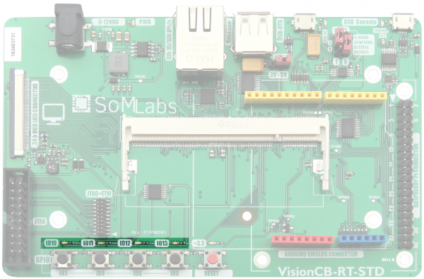
| LED | PCB designation | MCU pin name | Description |
|---|---|---|---|
| D400/blue | GPIO10 | GPIO_AD_B0_08 | Default: JTAG MOD input or universal GPIO with 3.3V logic levels. |
| D401/green | GPIO11 | GPIO_AD_B0_06 | Default: JTAG TMS input or universal GPIO with 3.3V logic levels. |
| D403/yellow | GPIO12 | GPIO_AD_B0_10 | Default: JTAG TDO input or universal GPIO with 3.3V logic levels. |
| D402/red | GPIO13 | GPIO_AD_B0_09 | Default: JTAG TDI input or universal GPIO with 3.3V logic levels. |
Notes:
1. LEDs are switched on by logic „1” set at the GPIO outputs.
2. LEDs are controlled by current drivers and do not load the GPIOs.
User switches connections
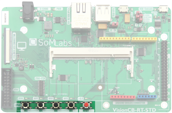
| Switch | PCB designation | MCU pin name | Description |
|---|---|---|---|
| S402 | GPIO3 | GPIO_AD_B0_03 | Universal GPIO with 3.3V logic levels. |
| S403 | GPIO4 | GPIO_AD_B0_04/BOOT0 | Universal GPIO with 3.3V logic levels. |
| S404 | GPIO8 | GPIO_AD_B1_09 | Universal GPIO with 3.3V logic levels. |
| S405 | GPIO9 | GPIO_B1_14 | Universal GPIO with 3.3V logic levels. |
Notes:
1. After button pressing on GPIO lines are set to „0”.
2. GPIO lines connected to switches are separated from board’s environment by 1k resistors.
TFT LCD connector (RGB 24b, J405)
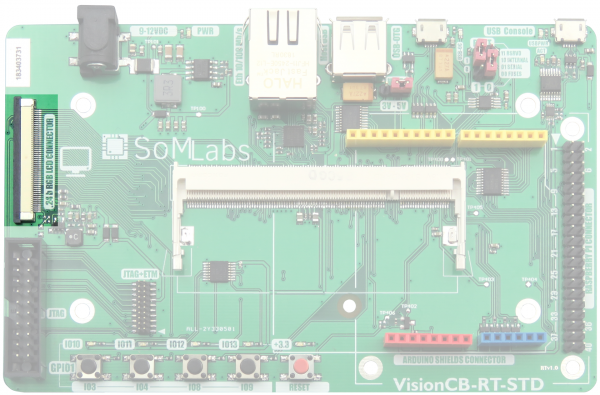
| J405 pin | Default function name | MCU pin name | LCD interface name |
|---|---|---|---|
| 1 | LCD-DATA0 | Internally connected to GND | LCD-B0 |
| 2 | LCD-DATA1 | Internally connected to GND | LCD-B1 |
| 3 | LCD-DATA2 | Internally connected to GND | LCD-B2 |
| 4 | LCD-DATA3 | GPIO_B0_04 | LCD-B3 |
| 5 | LCD-DATA4 | GPIO_B0_05 | LCD-B4 |
| 6 | LCD-DATA5 | GPIO_B0_06 | LCD-B5 |
| 7 | LCD-DATA6 | GPIO_B0_07 | LCD-B6 |
| 8 | LCD-DATA7 | GPIO_B0_08 | LCD-B7 |
| 9 | GND | - | GND |
| 10 | LCD-DATA8 | Internally connected to GND | LCD-G0 |
| 11 | LCD-DATA9 | Internally connected to GND | LCD-G1 |
| 12 | LCD-DATA10 | GPIO_B0_09 | LCD-G2 |
| 13 | LCD-DATA11 | GPIO_B0_10 | LCD-G3 |
| 14 | LCD-DATA12 | GPIO_B0_11 | LCD-G4 |
| 15 | LCD-DATA13 | GPIO_B0_12 | LCD-G5 |
| 16 | LCD-DATA14 | GPIO_B0_13 | LCD-G6 |
| 17 | LCD-DATA15 | GPIO_B0_14 | LCD-G7 |
| 18 | GND | - | GND |
| 19 | LCD-DATA16 | Internally connected to GND | LCD-R0 |
| 20 | LCD-DATA17 | Internally connected to GND | LCD-R1 |
| 21 | LCD-DATA18 | Internally connected to GND | LCD-R2 |
| 22 | LCD-DATA19 | GPIO_B0_15 | LCD-R3 |
| 23 | LCD-DATA20 | GPIO_B1_00 | LCD-R4 |
| 24 | LCD-DATA21 | GPIO_B1_01 | LCD-R5 |
| 25 | LCD-DATA22 | GPIO_B1_02 | LCD-R6 |
| 26 | LCD-DATA23 | GPIO_B1_03 | LCD-R7 |
| 27 | GND | - | GND |
| 28 | LCD-DE | GPIO_B0_01 | DE |
| 29 | LCD-HSYNC | GPIO_B0_02 | HSYNC |
| 30 | LCD-VSYNC | GPIO_B0_03 | VSYNC |
| 31 | GND | - | GND |
| 32 | LCD-PCLK | GPIO_B0_00 | DCLK |
| 33 | GND | - | GND |
| 34 | GPIO4 | GPIO_AD_B0_04 | TS-YPUL |
| 35 | GPIO3 | GPIO_AD_B0_03 | TS-YNUR |
| 36 | GPIO2 | GPIO_AD_B0_02 | TS-YPLL |
| 37 | GPIO1 | GPIO_AD_B0_00 | TS-YNLR |
| 38 | - | - | - |
| 39 | - | - | - |
| 40 | - | - | - |
| 41 | - | - | - |
| 42 | UART5-TXD | GPIO_B1_12 | I2C-SCL |
| 43 | UART5-RXD | GPIO_B1_13 | I2C-SDA |
| 44 | GND | - | GND |
| 45 | VCC-LCD | - | +3.3V (controlled by ENET2_TXEN) |
| 46 | VCC-LCD | - | +3.3V (controlled by ENET2_TXEN) |
| 47 | VCC-5V0 | - | +5.0V |
| 48 | VCC-5V0 | - | +5.0V |
| 49 | LCD-RESET | GPIO_AD_B1_08 | RESET |
| 50 | JTAG-nTRST | GPIO_AD_B0_11 | PWREN |
Dimensions
