StarCB-6ULL-STD Datasheet and Pinout
From SomLabs Wiki

StarCB-6ULL-STD Datasheet and Pinout
General description
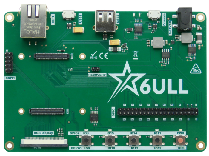
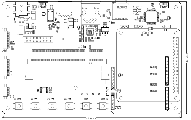
StarCB-6ULL-STD is a carrier board for the StarSOM-6ULL family of computer-on-modules, which are powered by NXP i.MX 6ULL application processors (ARM Cortex-A7). A carrier board, together with a System on Module (SoM), makes a complete development platform similar to SBC. The carrier board houses the most common interfaces such as USB, Ethernet, etc. A large variety of interfaces allows to use it as both a complete development platform or as a stand-alone end-product.
The carrier board connects with the SoM via a board-to-board, low profile connectors.
Applications
- IoT Sensor Hubs
- Home Appliances
- IoT gateways
- Protocol converters
- Home Automation – Smart Home
- Point-of-sales (POS) terminals
- Cash Register
- 2D barcode scanners and printers
- Smart grid infrastructure
- Residential gateways
- Outdoor equipment
Features
- Carrier Board (Base Board) compatible with the StarSOM-6ULL family of modules based iMX6ULL application processors
- SoM Interface: 2x100 board-to-board connectors
- Debug Interface: Linux console (vCOM/USB)
- Expansion Connectors:
- QSPI connector 2x10 Pin Header (Male)
- GPIO connector 2x20 Pin Header (Male)
- Communication Connectors:
- 1x Ethernet 10/100Mbit/s, RJ45
- 1x USB Host Type A connectors
- 1x USB OTG Micro AB connector
- 1x Console MicroUSB B connector
- Display Interface:
- 50-pin FFC/FPC parallel RGB (up to 24 bits)
- User Interface:
- 4+1 Pushbuttons
- 4+3 LEDs
- External Power Supply 9-12V DC
- Temperature Range: 0 to +70°C
- Board Size: 130mm x 90mm x 20mm
Pictures of StarCB-6LLL-STD board
| Version | Photo |
|---|---|
| StarCB-6LL-STD board only |
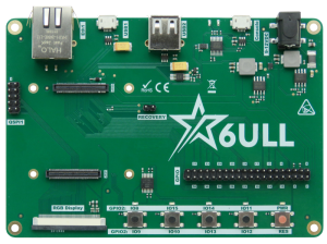 |
| StarCB-6LL-STD board - bottom side |
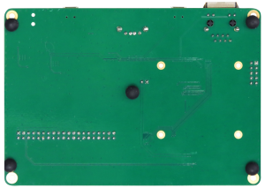 |
| StarCB-6LL-STD board with StarSOM-6ULL installed |
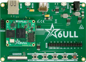 |
Ordering info
Block Diagram
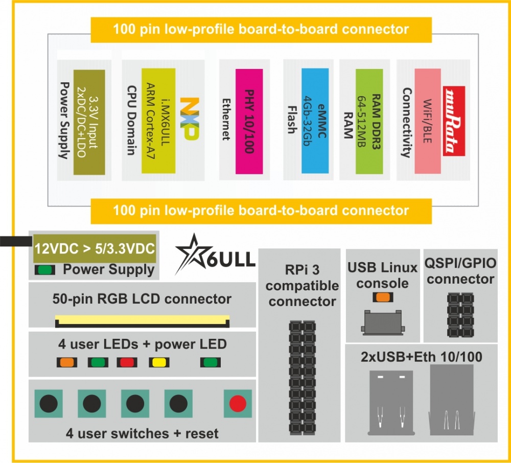
Electrical parameters
| Parameter | Value | Units | Comment | ||
|---|---|---|---|---|---|
| Min. | Typ. | Max. | |||
| Power Supply | 9.0 | 12.0 | 15.0 | V | Positive pole on central connector of J400 |
| Supply current | - | - | 0.09 | A | Excluding SOM, LCD, USB and antoher external loads |
| GPIO voltage | 3.3/5 | V | |||
QSPI interface (J502, 2x5 gold-pin, 2.54mm)
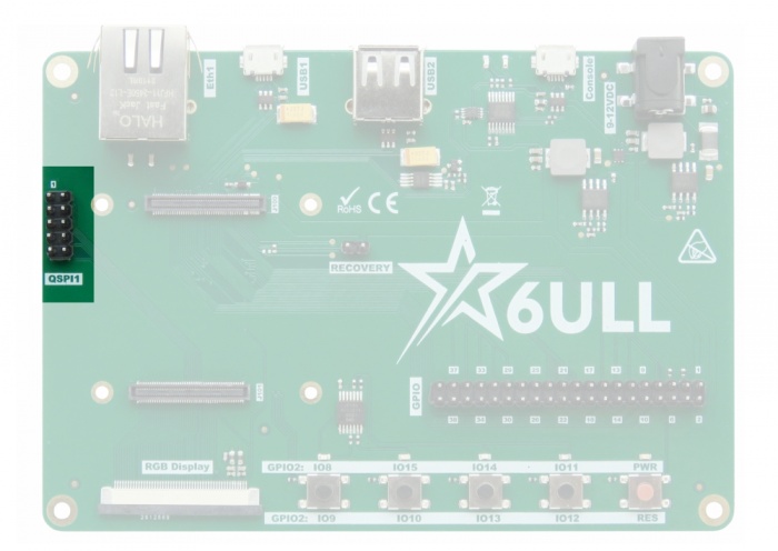
| Pin | Signal | Description |
|---|---|---|
| 1 | QSPI1.D0 | optionally GPIO4.12 |
| 2 | VDD-EMMC | Internal (on SOM) 1.8V LDO output as reference or power supply voltage for QSPI (SDIO) interface |
| 3 | QSPI1.D1 | optionally GPIO4.13 |
| 4 | QSPI1.CS0 | optionally GPIO4.16 |
| 5 | QSPI1.D2 | optionally GPIO4.14 |
| 6 | QSPI1.CLK | optionally GPIO4.11 |
| 7 | QSPI1.D3 | optionally GPIO4.15 |
| 8 | - | - |
| 9 | QSPI1.DQS | optionally GPIO4.10 |
| 10 | GND | - |
GPIO connector (J500, 2x20 gold-pin, 2.54mm)
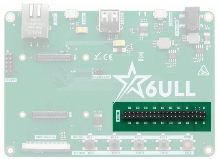
| Pin | Signal | Description |
|---|---|---|
| 1 | VDD-3V3 | Power supply for external loads (up to 300 mA) |
| 2 | VDD-5V0 | Power supply for external loads (up to 200 mA) |
| 3 | I2C2-SDA | 4.7k pull-up resistor connected Connected to LCD J300 connector (touch panel controller) Optionally GPIO1.31 |
| 4 | VDD-5V0 | Power supply for external loads (up to 200 mA) |
| 5 | I2C2-SCL | 4.7k pull-up resistor connected Connected to LCD J300 connector (touch panel controller) Optionally GPIO1.30 |
| 6 | GND | - |
| 7 | TAMPER.0 | optionally GPIO5.00 |
| 8 | UART3.TXD | optionally GPIO1.24 |
| 9 | GND | - |
| 10 | UART3.RXD | optionally GPIO1.25 |
| 11 | TAMPER.1 | optionally GPIO5.01 |
| 12 | UART3.RTS | optionally GPIO1.27 |
| 13 | TAMPER.2 | optionally GPIO5.02 |
| 14 | GND | - |
| 15 | TAMPER.3 | optionally GPIO5.03 |
| 16 | UART3.CTS | optionally GPIO1.26 |
| 17 | VDD-3V3 | Power supply for external loads (up to 300 mA) |
| 18 | JTAG.TDI | optionally GPIO1.13 |
| 19 | UART1.CTS | optionally GPIO1.18 |
| 20 | GND | - |
| 21 | UART1.RTS | optionally GPIO1.19 |
| 22 | JTAG.TMS | optionally GPIO1.11 |
| 23 | UART1.RXD | optionally GPIO1.17 |
| 24 | UART1.TXD | optionally GPIO1.16 |
| 25 | GND | - |
| 26 | TAMPER.9 | optionally GPIO5.09 |
| 27 | - | - |
| 28 | - | - |
| 29 | TAMPER.4 | optionally GPIO5.04 |
| 30 | GND | - |
| 31 | UART2.RXD | optionally GPIO1.21 |
| 32 | TAMPER.8 | optionally GPIO5.08 |
| 33 | UART2.TXD | optionally GPIO1.20 |
| 34 | GND | - |
| 35 | UART2.RTS | optionally GPIO1.23 |
| 36 | TAMPER.7 | optionally GPIO5.07 |
| 37 | UART2.CTS | optionally GPIO1.22 |
| 38 | TAMPER.6 | optionally GPIO5.06 |
| 39 | GND | - |
| 40 | TAMPER.5 | optionally GPIO5.05 |
Display interface (J300, FPC/FFC 0.5mm)
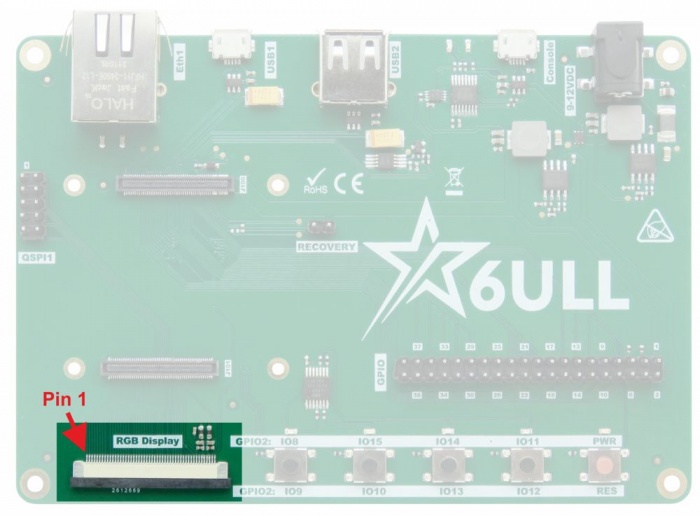
| Pin | Signal | Description |
|---|---|---|
| 1 | LCD.DATA00 | B0 |
| 2 | LCD.DATA01 | B1 |
| 3 | LCD.DATA02 | B2 |
| 4 | LCD.DATA03 | B3 |
| 5 | LCD.DATA04 | B4 |
| 6 | LCD.DATA05 | B5 |
| 7 | LCD.DATA06 | B6 |
| 8 | LCD.DATA07 | B7 |
| 9 | GND | - |
| 10 | LCD.DATA08 | G0 |
| 11 | LCD.DATA09 | G1 |
| 12 | LCD.DATA10 | G2 |
| 13 | LCD.DATA11 | G3 |
| 14 | LCD.DATA12 | G4 |
| 15 | LCD.DATA13 | G5 |
| 16 | LCD.DATA14 | G6 |
| 17 | LCD.DATA15 | G7 |
| 18 | GND | - |
| 19 | LCD.DATA16 | R0 |
| 20 | LCD.DATA17 | R1 |
| 21 | LCD.DATA18 | R2 |
| 22 | LCD.DATA19 | R3 |
| 23 | LCD.DATA20 | R4 |
| 24 | LCD.DATA21 | R5 |
| 25 | LCD.DATA22 | R6 |
| 26 | LCD.DATA23 | R7 |
| 27 | GND | - |
| 28 | LCD.ENABLE | - |
| 29 | LCD.HSYNC | - |
| 30 | LCD.VSYNC | - |
| 31 | GND | - |
| 32 | LCD.CLK | - |
| 33 | GND | - |
| 34 | GPIO1.04 | TS-YPUL |
| 35 | GPIO1.03 | TS-YNUR |
| 36 | GPIO1.02 | TS-YPLL |
| 37 | GPIO1.01 | TS-YNLR |
| 38 | - | - |
| 39 | - | - |
| 40 | - | - |
| 41 | - | - |
| 42 | I2C2-SCL | 4.7k pull-up resistor connected Touch panel controller interface |
| 43 | I2C2-SDA | 4.7k pull-up resistor connected Touch panel controller interface |
| 44 | GND | - |
| 45 | VDD-3V3 | +3.3V power source fr LCD module |
| 46 | VDD-3V3 | +3.3V power source fr LCD module |
| 47 | VDD-3V3 | +3.3V power source fr LCD module |
| 48 | VDD-3V3 | +3.3V power source fr LCD module |
| 49 | LCD.RESET | Optional reset signal GPIO3.04 |
| 50 | PWREN | Optional power-enable signal GPIO1.15 |
USB Console Port
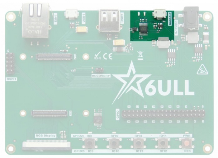
| MPU Port | GPIO | Description |
|---|---|---|
| CONSOLE-TXD | UART4-TXD | - |
| CONSOLE-RXD | UART4-RXD | - |
Note:
1. Linux console port (UART4 in MPU) uses vCOM interface.
MicroSD card interface (J308)
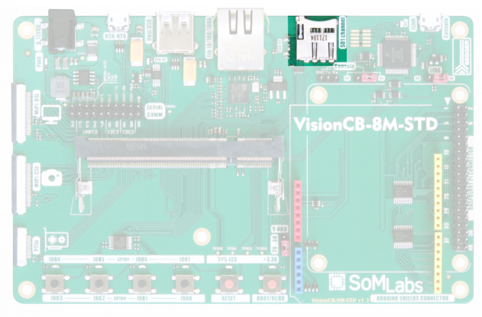
| Connector pin | SD card signal | SOM pin |
|---|---|---|
| 1 | DATA2 | SD1-DATA2 |
| 2 | DATA3 | SD1-DATA3 |
| 3 | CMD | SD1-CMD |
| 4 | NVCC-SDIO | Voltage selected 1.8/3.3V by SD1 driver |
| 5 | CLK | SD1-CLK |
| 6 | GND | - |
| 7 | DATA0 | SD1-DATA0 |
| 8 | DATA1 | SD1-DATA1 |
| 9 | CARD-DETECT | SD1-CD |
Raspberry Pi compatible I/O header
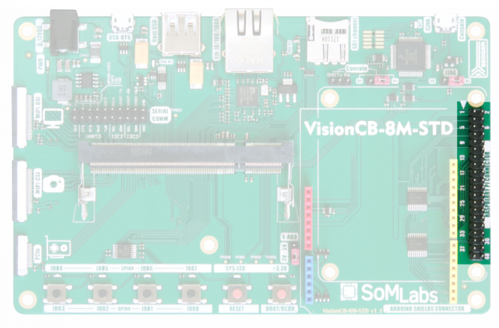
| Pin | Default function name | Description |
|---|---|---|
| 1 | +3.3V | +3.3V generated by DC/DC built-in SOM (limited current load) |
| 2 | +5V | +5V generated by carrier board built-in DC/DC converter |
| 3 | I2C1-SDA | I2C1-SDA line |
| 4 | +5V | +5V generated by carrier board built-in DC/DC converter |
| 5 | I2C1-SDA | I2C1-SDA line |
| 6 | GND | - |
| 7 | GPIO4-IO09 | Universal GPIO with 3.3V logic levels |
| 8 | UART3-TXD | Default: UART3 TXD line or universal GPIO with 3.3V logic levels |
| 9 | GND | - |
| 10 | UART3-RXD | Default: UART3 RXD line or universal GPIO with 3.3V logic levels |
| 11 | GPIO4-IO08 | Universal GPIO with 3.3V logic levels |
| 12 | SPI2-CLK | Default: SPI2-CLK line or universal GPIO with 3.3V logic levels |
| 13 | - | - |
| 14 | GND | - |
| 15 | - | - |
| 16 | SPI2-MISO | Default: SPI2-MISO line or universal GPIO with 3.3V logic levels |
| 17 | +3.3V | +3.3V generated by DC/DC built-in SOM (limited current load) |
| 18 | SPI2-MOSI | Default: SPI2-MOSI line or universal GPIO with 3.3V logic levels |
| 19 | SPI1-MOSI | Default: SPI1-MOSI line or universal GPIO with 3.3V logic levels |
| 20 | GND | - |
| 21 | SPI1-MISO | Default: SPI1-MISO line or universal GPIO with 3.3V logic levels |
| 22 | SPI2-SS0 | Default: SPI2-SS0 line or universal GPIO with 3.3V logic levels |
| 23 | SPI1-CLK | Default: SPI1-CLK line or universal GPIO with 3.3V logic levels |
| 24 | SPI1-SS0 | Default: SPI1-SS0 line or universal GPIO with 3.3V logic levels |
| 25 | GND | - |
| 26 | GPIO-IO22 | Universal GPIO with 3.3V logic levels |
| 27 | - | - |
| 28 | - | - |
| 29 | GPIO4-IO12 | Universal GPIO with 3.3V logic levels |
| 30 | GND | - |
| 31 | GPIO4-IO13 | Universal GPIO with 3.3V logic levels |
| 32 | GPIO4-IO20 | Universal GPIO with 3.3V logic levels |
| 33 | GPIO4-IO14 | Universal GPIO with 3.3V logic levels |
| 34 | GND | - |
| 35 | GPIO4-IO14 | Universal GPIO with 3.3V logic levels |
| 36 | GPIO4-IO19 | Universal GPIO with 3.3V logic levels |
| 37 | GPIO4-IO16 | Universal GPIO with 3.3V logic levels |
| 38 | GPIO4-IO18 | Universal GPIO with 3.3V logic levels |
| 39 | GND | - |
| 40 | GPIO4-IO17 | Universal GPIO with 3.3V logic levels |
Arduino Uno compatible I/O header
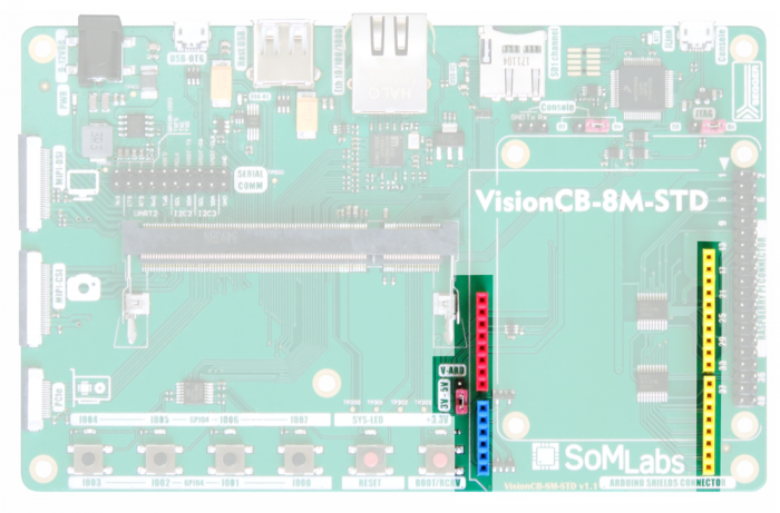
| Pin | Arduino name | Default function name | Description |
|---|---|---|---|
| Power connector J700, red connector | |||
| 1 | - | - | - |
| 2 | IOREF | VDD-ARDUINO-IO | Selected +3.3V or +5V (with V-ARD jumper). |
| 3 | RESET | POR-B | External reset input, active L. |
| 4 | 3.3V | VCC-3V3 | +3.3V generated by internal SOM LDO converter (limited load current). |
| 5 | 5V | VCC-5V0 | +5V generated by carrier board built-in DC/DC converter. |
| 6 | GND | GND | - |
| 7 | GND | GND | - |
| 8 | VIN | VCC-3V3 | +3.3V generated by internal SOM LDO converter (limited load current). |
| Analog inputs connector J702, blue connector | |||
| 1 | AIN0 | - | Not internally connected. |
| 2 | AIN1 | - | Not internally connected. |
| 3 | AIN2 | - | Not internally connected. |
| 4 | AIN3 | - | Not internally connected. |
| 5 | - | - | Not internally connected. |
| 6 | - | - | Not internally connected. |
| Digital I/Os connector J704, yellow connector | |||
| 1 | DIO0 | UART3-RXD | Default: UART3-RXD line or universal GPIO with 3.3/5V logic levels. |
| 2 | DIO1 | UART3-TXD | Default: UART3-TXD line or universal GPIO with 3.3/5V logic levels. |
| 3 | DIO2 | GPIO4-IO15 | Universal GPIO with 3.3/5V logic levels. |
| 4 | DIO3 | GPIO4-IO14 | Universal GPIO with 3.3/5V logic levels. |
| 5 | DIO4 | GPIO4-IO13 | Universal GPIO with 3.3/5V logic levels. |
| 6 | DIO5 | GPIO4-IO12 | Universal GPIO with 3.3/5V logic levels. |
| 7 | DIO6 | GPIO4-IO11 | Universal GPIO with 3.3/5V logic levels. |
| 8 | DIO7 | GPIO4-IO10 | Universal GPIO with 3.3/5V logic levels. |
| Digital I/Os connector J703, yellow connector | |||
| 1 | DIO8 | GPIO4-IO08 | Universal GPIO with 3.3/5V logic levels. |
| 2 | DIO9 | GPIO4-IO09 | Universal GPIO with 3.3/5V logic levels. |
| 3 | DIO10 | SPI1-SS0 | Default: SPI1-SS0 line or universal GPIO with 3.3/5V logic levels. |
| 4 | DIO11 | SPI1-MOSI | Default: SPI1-MOSI line or universal GPIO with 3.3/5V logic levels. |
| 5 | DIO12 | SPI1-MISO | Default: SPI1-MISO line or universal GPIO with 3.3/5V logic levels. |
| 6 | DIO13 | SPI1-CLK | Default: SPI1-CLK line or universal GPIO with 3.3/5V logic levels. |
| 7 | GND | GND | - |
| 8 | AREF | VDD-ARDUINO-IO | +3.3V or +5V selected with V-ARD jumper. |
| 9 | DIO14 | I2C1-SCL | Default: I2C1-SCL line or universal GPIO with 3.3/5V logic levels. |
| 10 | DIO15 | I2C1-SDA | Default: I2C1-SDA line or universal GPIO with 3.3/5V logic levels. |
Notes:
1. I/O logic levels are selected 3.3/5V with V-ARD jumper.
2. RESET line is 3.3 and 5V compatible.
Serial Communication/GPIO header (J305)
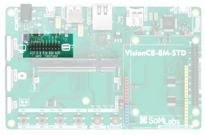
| Pin | Default function name | Description |
|---|---|---|
| 1 | +3.3V | +3.3V generated by DC/DC built-in SOM (limited current load) |
| 2 | GPIO5-IO23 | Universal GPIO with 3.3V logic levels By default is connected to MIPI-DSI (J301) as touch-panel interrupt line (with 47k pull-up) |
| 3 | UART2-CTS | By default: UART2-CTS or universal GPIO with 3.3V logic levels |
| 4 | SAI3-TXFS | By default: SAI3-TXFS or universal GPIO with 3.3V logic levels Connected to MIPI-CSI (J302) |
| 5 | UART2-RTS | By default: UART2-RTS or universal GPIO with 3.3V logic levels |
| 6 | SAI3-TXC | By default: SAI3-TXC or universal GPIO with 3.3V logic levels Connected to MIPI-CSI (J302) |
| 7 | UART2-RXD | By default: UART2-RXD or universal GPIO with 3.3V logic levels |
| 8 | SAI3-TXD | By default: SAI3-TXD or universal GPIO with 3.3V logic levels |
| 9 | UART2-TXD | By default: UART2-TXD or universal GPIO with 3.3V logic levels |
| 10 | SAI3-RXFS | By default: SAI3-RXFS or universal GPIO with 3.3V logic levels By default is connected to MIPI-DSI (J301) as display module reset signal |
| 11 | I2C2-SCL | By default: I2C2-SCL or universal GPIO with 3.3V logic levels Default I2C port for PCIe (J303), MIPI-DSI (J301) and MIPI-CSI (J302) |
| 12 | SAI3-MCLK | By default: SAI3-MCLK or universal GPIO with 3.3V logic levels |
| 13 | I2C2-SDA | By default: I2C2-SDA or universal GPIO with 3.3V logic levels Default I2C port for PCIe (J303), MIPI-DSI (J301) and MIPI-CSI (J302) |
| 14 | SPDIF-TX | By default: SPDIC-TX or universal GPIO with 3.3V logic levels By default is connected to MIPI-DSI (J301) as touch-panel reset signal |
| 15 | I2C3-SCL | By default: I2C3-SCL or universal GPIO with 3.3V logic levels |
| 16 | SPDIF-RX | By default: I2C3-SCL or universal GPIO with 3.3V logic levels By default is connected to MIPI-DSI (J301) as display module PWM backlight control |
| 17 | I2C3-SDA | By default: I2C3-SDA or universal GPIO with 3.3V logic levels |
| 18 | SPDIF-CLK | By default: SPDIF-CLK or universal GPIO with 3.3V logic levels By default is connected to MIPI-DSI (J301) as display module on/off signal |
| 19 | GND | - |
| 20 | GND | - |
User Interface (switches and LEDs)
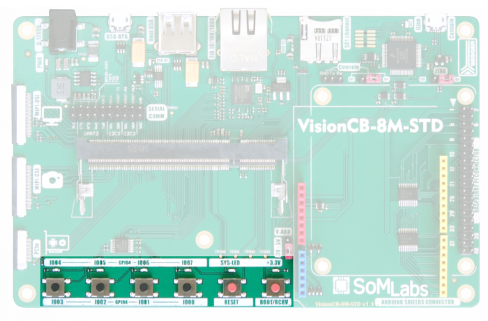
User switches
| Switch | GPIO | Description |
|---|---|---|
| S305 (black, most on the left) | GPIO4-IO03 | 47k pull-up |
| S304 | GPIO4-IO02 | 47k pull-up |
| S303 | GPIO4-IO01 | 47k pull-up |
| S302 (black, most on the right) | GPIO4-IO00 | 47k pull-up |
System switches
| Switch | Signal name | Description |
|---|---|---|
| S301 (left, red) | Reset | - |
| S300 (right, red) | BOOT-RECOVERY | - |
User LEDs
| LED | GPIO | Description |
|---|---|---|
| D303 (most on the left) | GPIO4-IO04 | User LED1, buffered with inverter |
| D302 | GPIO4-IO05 | User LED2, buffered with inverter |
| D301 | GPIO4-IO06 | User LED3, buffered with inverter |
| D300 (most on the right) | GPIO4-IO07 | User LED4, buffered with inverter |
System LEDs
| LED | GPIO | Description |
|---|---|---|
| D304 | SYS-LED | System function monitoring |
| D305 | - | Power LED (3.3V) |
Dimensions
