VisionSOM-V2L Datasheet and Pinout
From SomLabs Wiki

VisionSOM-V2L Datasheet and Pinout
General description
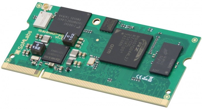
The VisionSOM-V2L family is a SODIMM-sized SoM based on the Renesas dual core RZ/V2L application processor which features an advanced implementation of DRP-AI (ML+AI) coprocessor. The VisionSOM-V2L family offers energy efficient dual ARM Cortex-A55 cores (at speed up to 1.2GHz) and ARM Cortex-M33 core (at speed up to 200MHz) as well as a 3D Graphics Processing Unit (ARM Mali-G31 GPU @500MHz, 1920x1080 @60fps) with Open GL 3.2ES/OpenCL 2.0 (Full Profile) capabilities and Video Codec Processor (VCP) with 1920x1080 @30fps.
The VisionSOM-V2L is a multimedia and video oriented, highly integrated SoM (System on Module) featuring high computation power, optinally integrated 2.4GHz Wi-Fi and Bluetooth v5.1 connectivity. The option of integrated, fully certified Wi-Fi and Bluetooth module simplifies the carrier board design and is ideally suited for wireless application. The VisionSOM-V2L provides a variety memory configuration, including 1GB of fast and efficient DDR4 and eMMC Flash that meets our customers requirements.
The SoM supports connections to a variety of interfaces: two high-speed USB 2.0 with integrated PHY, dual Ethernet 1Gbit, audio, MIPI-DSI display output with optional touch panel, MIPI-CSI camera input with scaling processor, serial communication interfaces including 2xCAN. In addition, the system supports industrial grade embedded applications.
SoMLabs also provides a complete hardware and software development board for the SoM in the form of a carrier board and optional TFT display and touch panel.
Applications
- IoT Edge Devices
- IoT gateways
- Machine vision equipment
- AI+ML Decision/Recognition Systems
- Robotics
- Human-machine Interfaces (HMI)
- IP Cameras
- Home Appliances
- Home Automation – Smart Home
- Residential gateways
- Industrial embedded Linux computer
- Fitness/outdoor equipment
Features
- Powered by dual core Renesas RZ/V2L application processor (R9A07G054L27GBG)
- Dual ARM Cortex-A55 core at speed up to 1.2GHz
- ARM Cortex-M33 core at speed up to 200MHz
- Integrated Machine-Learning (ML) and Artificial Intelligence (AI) AI Accelerator (DRP-AI)
- Integrated 3D GPU (ARM Mali-G31 @500MHz)
- 1GB RAM (DDR4)
- Up to 32GB eMMC memory
- Optional Murata radio module 2.4GHz Wi-Fi and Bluetooth v5.1
- Built-in dual USB 2.0 interface
- Built-in 2xCAN-FD interfaces
- Built-in MIPI-DSI display interface
- Built-in MIPI-CSI camera interface
- Power-efficient and cost-optimized solution
- Ideal for industrial IoT and embedded applications
- Integrated security features
Pictures of SOM versions
| Version | Photo |
|---|---|
| eMMC |
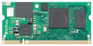 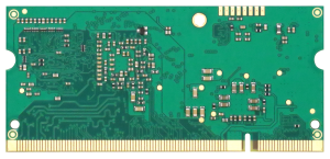 |
| WiFi/BT module is available for all memory configurations. |
Ordering info
| SLS | Product type SLS - System on Module |
| 2 | SOM Name 2 - High Performance VisionSOM SODIM200 module |
| 2 | CPU Family 2 - Renesas RZ/V2L family |
| CpuType | CPU Type RV2LDC - RZ/V2L dual Cortex-A55 + Cortex-M33 + DRP-AI |
| Clock | CPU Clock Speed 1200C - 1.2GHz |
| RamSize | DDR4 RAM Size 01GR - 1GB (1024MB) |
| FlashSize | eMMC Memory Size 04GE - 4GB eMMC 08GE - 8GB eMMC 16GE - 16GB eMMC 32GE - 32GB eMMC |
| SF | Special Features 0SF - No Special Features 1WB - Built-in 2.4GHz Wi-Fi and Bluetooth v5.1 |
| TEMP | Operating Temperature E - Extended: -25 to +70 C I - Industrial: -40 to +85 C |
Block Diagram
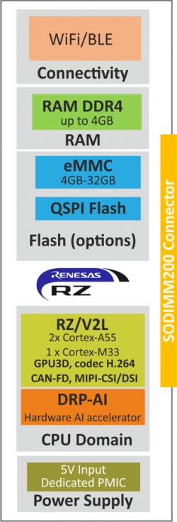
Operating ranges
| Parameter | Value | Unit | Comment |
|---|---|---|---|
| Power Supply | Connected to VDD 5V SODIM260 pins | ||
| Max. input GPIO voltage | - | ||
| Environment temperature1 | oC | Industrial range w/o WiFi module | |
| Industrial range with WiFi module | |||
| Consumer range |
Note:
1. Maximum MPU junction temperature is +105oC.
2. Junction temperature determines MPU lifetime. Details: NXP AN13214 Application Note.
Electrical parameters
| SOM signal name |
Parameter | Value | Unit | ||
|---|---|---|---|---|---|
| Min. | Typ. | Max. | |||
| VDD-5V | Supply Voltage (Input) | 4.0 | 5.0 | 5.25 | V |
| SD1-NVCC | Output power supply for external 1.8/3.3V accesories | - | - | 0.08 | A |
| VDD-1V8 | Output power supply for external 1.8V accesories | - | - | 0.4 | A |
| VDD-3V3 | Output power supply for external 3.3V accesories | - | - | 0.31 | A |
| VGPIO @1V8 | GPIO Input Voltage | 0 | - | 2.05 | V |
| VGPIO @3V3 | GPIO Input Voltage | 0 | - | 3.62 | V |
| VUSB_VBUS | USB VBUS Input Voltage | 0 | - | 3.953 | V |
Notes:
1. Total current on both VDD-3V3 outputs.
2. Applying the maximum voltage 3.6V results in shorten lifetime. Recommended value is smaller than 3.45V.
3. Input current is limited by 30k resistor connected in series.
SoM pinout
Important notes:
1. Detail pin configurations description you can find, edit and arrange in dedicated MEX file (with free "iMX PinTool" configurational tool).
2. JTAG-MOD (ball G2) is permanently connected to GND
3. BOOT-MODE0 – RECOVERY line 0 -> BOOT-MODE0=1
4. BOOT-MODE1...MODE3 are premanently connected to GND
5. SDIO2 interface is used to communication with Murata 1ZM radio module
6. eMMC memory is connected to SDIO3 interface
| SOM pin numer | Default function | GPIO | BGA456 ball | Notes |
|---|---|---|---|---|
| 1 | GND | Power | - | |
| 2 | GND | Power | - | |
| 3 | ET0-PHY-RST | P47-1 | A20 | 1.8V Power Domain GPIO mode not allowed |
| 4 | PWR-GOOD | Output | PMIC power-good signalling for external devices | |
| 5 | ET0-INT | P47-0 | B20 | 3.3V Power Domain |
| 6 | PWR-ON | Input | PMIC PWRON input (on-off function) Internal pull-down Connect to GND if not used Connect to VDD-3V3 with external pull-up resistor (4.7kOhm) and pushbutton to GND if used | |
| 7 | ET0-MDIO | I/O | U1 | 1.8V Power Domain GPIO mode not allowed |
| 8 | PWR-FAIL | Input | PMIC enable-input: PWR-FAIL='0' -> SOM power supply is off PWR-FAIL='1' or left open -> SOM power supply is on Can bue used as cold-reset input (active low) | |
| 9 | ET0-MDC | I/O | U2 | 1.8V Power Domain GPIO mode not allowed |
| 10 | RESET-OUT | Output | RESET output for external peripherals | |
| 11 | GND | Power | - | |
| 12 | RESET-IN | Input | MPU reset input, active low | |
| 13 | ET0-RXC | I/O | P2 | 1.8V Power Domain GPIO mode not allowed |
| 14 | GND | Power | - | |
| 15 | ET0-RX-CTL | I/O | P1 | 1.8V Power Domain GPIO mode not allowed |
| 16 | UART0-RXD | P38-1 | B15 | 3.3V Power Domain |
| 17 | ET0-RXD0 | I/O | R2 | 1.8V Power Domain GPIO mode not allowed |
| 18 | UART0-TXD | P38-0 | A15 | 3.3V Power Domain |
| 19 | ET0-RXD1 | I/O | R1 | 1.8V Power Domain GPIO mode not allowed |
| 20 | UART1-CTS | P41-0 | E17 | 3.3V Power Domain |
| 21 | ET0-RXD2 | I/O | T2 | 1.8V Power Domain GPIO mode not allowed |
| 22 | UART1-RTS | P41-1 | A18 | 3.3V Power Domain |
| 23 | ET0-RXD3 | I/O | T1 | 1.8V Power Domain GPIO mode not allowed |
| 24 | UART1-RXD | P40-0 | C17 | 3.3V Power Domain |
| 25 | GND | Power | - | |
| 26 | UART1-TXD | P40-1 | B17 | 3.3V Power Domain |
| 27 | ET0-TX-CTL | I/O | N2 | 1.8V Power Domain GPIO mode not allowed |
| 28 | UART4-RXD | P2-1 | A13 | 3.3V Power Domain |
| 29 | ET0-TXC | I/O | N1 | 1.8V Power Domain GPIO mode not allowed |
| 30 | UART4-TXD | P2-0 | B13 | 3.3V Power Domain |
| 31 | ET0-TXD3 | I/O | N1 | 1.8V Power Domain GPIO mode not allowed |
| 32 | UART3-RXD | P0-1 | B12 | 3.3V Power Domain |
| 33 | ET0-TXD2 | I/O | L2 | 1.8V Power Domain GPIO mode not allowed |
| 34 | UART3-TXD | P0-0 | A11 | 3.3V Power Domain |
| 35 | ET0-TXD1 | I/O | M2 | 1.8V Power Domain GPIO mode not allowed |
| 36 | VBAT-RTC | Power | - | RTC 3V battery |
| 37 | ET0-TXD0 | I/O | M1 | 1.8V Power Domain GPIO mode not allowed |
| 38 | GND | Power | - | |
| 39 | VDD-1V8 | Power | 1.8V output for external devices, max. 300 mA | |
| 40 | VDD-1V8 | Power | 1.8V output for external devices, max. 300 mA | |
| 41 | VDD-5V0 | Power | External power supply | |
| 42 | VDD-5V0 | Power | External power supply | |
| 43 | VDD-5V0 | Power | External power supply | |
| 44 | VDD-5V0 | Power | External power supply | |
| 45 | VDD-5V0 | Power | External power supply | |
| 46 | VDD-5V0 | Power | External power supply | |
| 47 | VDD-5V0 | Power | External power supply | |
| 48 | VDD-5V0 | Power | External power supply | |
| 49 | VDD-5V0 | Power | External power supply | |
| 50 | VDD-5V0 | Power | External power supply | |
| 51 | NC | Not Connected | - | |
| 52 | NC | Not Connected | - | |
| 53 | VDD-3V3 | Power | 3.3V output for external devices, max. 300mA | |
| 54 | VDD-3V3 | Power | - | 3.3V output for external devices, max. 300mA |
| 55 | GND | Power | - | |
| 56 | SYSLED | P42-0 | AG4 | 3.3V Power Domain |
| 57 | VPROG | NC | - | For SoMLabs purposes only, leave unconnected |
| 58 | GND | Power | - | |
| 59 | BOOT-RECOVERY | Input | BOOT input, active low during reset | |
| 61 | GND | Power | - | |
| 62 | SSI0-RXD | P7-1 | AH28 | 3.3V Power Domain |
| 63 | ET1-VDD-SEL | Input | Ethernet 1 (ET1) interface voltage selection: ET1-VDD-SEL='0' -> V=1.8V ET1-VDD-SEL='1' or left open -> V=3.3V The line has internal pull-up. | |
| 64 | SSI0-TXD | P7-0 | AJ28 | 3.3V Power Domain |
| 65 | ET1-PHY-RST | P47-3 | B21 | 3.3V Power Domain |
| 66 | SSI0-RCK | P6-1 | AH27 | 3.3V Power Domain |
| 67 | ET1-INT | P47-2 | A21 | 3.3V Power Domain |
| 68 | SSI0-BCK | P6-0 | AJ27 | 3.3V Power Domain |
| 69 | ET1-MDIO | P37-1 | W1 | 1.8V or 3.3V Power Domain selected by ET1-VDD-SEL GPIO allowed only for 3.3V. |
| 70 | GND | Power | - | |
| 71 | ET1-MDC | P37-0 | W2 | 1.8V or 3.3V Power Domain selected by ET1-VDD-SEL GPIO allowed only for 3.3V. |
| 72 | CAN1-RX | P13-0 | AF23 | 3.3V Power Domain |
| 73 | GND | Power | - | |
| 74 | CAN1-TX | P12-1 | AE23 | 3.3V Power Domain |
| 75 | ET1-RXC | P33-1 | AC1 | 1.8V or 3.3V Power Domain selected by ET1-VDD-SEL GPIO allowed only for 3.3V. |
| 76 | CAN0-RX | P42-2 | AJ3 | 3.3V Power Domain |
| 77 | ET1-RX-CTL | P34-0 | AC2 | 1.8V or 3.3V Power Domain selected by ET1-VDD-SEL GPIO allowed only for 3.3V. |
| 78 | CAN0-TX | P42-1 | AE7 | 3.3V Power Domain |
| 79 | ET1-RXD0 | P34-1 | AC3 | 1.8V or 3.3V Power Domain selected by ET1-VDD-SEL GPIO allowed only for 3.3V. |
| 80 | GND | Power | - | |
| 81 | ET1-RXD1 | P35-0 | AC4 | 1.8V or 3.3V Power Domain selected by ET1-VDD-SEL GPIO allowed only for 3.3V. |
| 82 | I2C3-SCL-EXT | P46-3 | D13 | I2C interface used for on-board PMIC configuration Built-in pull-up resistor 2.2kOhm connected to 3.3V 3.3V Power Domain |
| 83 | ET1-RXD2 | P35-1 | AB4 | 1.8V or 3.3V Power Domain selected by ET1-VDD-SEL GPIO allowed only for 3.3V. |
| 84 | I2C3-SDA-EXT | P46-2 | C12 | I2C interface used for on-board PMIC configuration Built-in pull-up resistor 2.2kOhm connected to 3.3V 3.3V Power Domain |
| 85 | ET1-RXD3 | P36-0 | AB3 | 1.8V or 3.3V Power Domain selected by ET1-VDD-SEL GPIO allowed only for 3.3V. |
| 86 | I2C2-SCL | P42-4 | AC5 | Built-in pull-up resistor 2.2kOhm connected to 3.3V |
| 87 | GND | Power | - | |
| 88 | I2C2-SDA | P42-3 | AH3 | Built-in pull-up resistor 2.2kOhm connected to 3.3V |
| 89 | ET1-TX-CTL | P29-1 | Y1 | 1.8V or 3.3V Power Domain selected by ET1-VDD-SEL GPIO allowed only for 3.3V. |
| 90 | P19-0 | P19-0 | B1 | 3.3V Power Domain |
| 91 | ET1-TXC | P29-0 | AB2 | 1.8V or 3.3V Power Domain selected by ET1-VDD-SEL GPIO allowed only for 3.3V. |
| 92 | P18-0 | P18-0 | C2 | 3.3V Power Domain |
| 93 | ET1-TXD3 | P31-1 | Y2 | 1.8V or 3.3V Power Domain selected by ET1-VDD-SEL GPIO allowed only for 3.3V. |
| 94 | GND | Power | - | |
| 95 | ET1-TXD2 | P31-0 | AA1 | 1.8V or 3.3V Power Domain selected by ET1-VDD-SEL GPIO allowed only for 3.3V. |
| 96 | P18-1 | P18-1 | D3 | 3.3V Power Domain |
| 97 | ET1-TXD1 | P30-1 | AA2 | 1.8V or 3.3V Power Domain selected by ET1-VDD-SEL GPIO allowed only for 3.3V. |
| 98 | P45-0 | P45-0 | A8 | 3.3V Power Domain |
| 99 | ET1-TXD0 | P30-0 | AB1 | 1.8V or 3.3V Power Domain selected by ET1-VDD-SEL GPIO allowed only for 3.3V. |
| 100 | P45-2 | P45-2 | A9 | 3.3V Power Domain |
| 101 | GND | Power | - | |
| 102 | P45-3 | P45-3 | B9 | 3.3V Power Domain |
| 103 | USB1-D_N | Analog I/O | - | |
| 104 | P46-0 | P46-0 | B10 | 3.3V Power Domain |
| 105 | USB1-D_P | Analog I/O | - | |
| 106 | P46-1 | P46-1 | A10 | 3.3V Power Domain |
| 107 | USB1-OC | P8-1 | AJ20 | 3.3V Power Domain |
| 108 | P45-1 | P45-1 | D12 | 3.3V Power Domain |
| 109 | USB1-EN | P8-0 | AH19 | 3.3V Power Domain |
| 110 | P1-1 | P1-1 | A12 | 3.3V Power Domain |
| 111 | GND | Power | - | |
| 112 | P3-1 | P3-1 | B14 | 3.3V Power Domain |
| 113 | USB0-OC | P5-0 | AJ4 | 3.3V Power Domain |
| 114 | P1-0 | P1-0 | C13 | 3.3V Power Domain |
| 115 | USB0-EN | P4-0 | AJ5 | 3.3V Power Domain |
| 116 | GND | Power | - | |
| 117 | USB0-ID | P5-1 | AH4 | 3.3V Power Domain |
| 118 | P3-0 | P3-0 | A14 | 3.3V Power Domain |
| 119 | USB0-D_N | Analog I/O | - | |
| 120 | P48-2 | P48-2 | A22 | 3.3V Power Domain |
| 121 | USB0-D_P | Analog I/O | - | |
| 122 | P4-1 | P4-1 | AH6 | 3.3V Power Domain |
| 123 | USB0-VBUS | Dedicated input | AH10 | 3.3V Power Domain |
| 124 | P7-2 | P7-2 | AJ19 | 3.3V Power Domain |
| 125 | GND | Power | - | |
| 126 | GND | Power | - | |
| 127 | P11-1 | P11-1 | AF22 | 3.3V Power Domain |
| 128 | P11-0 | P11-0 | AG22 | 3.3V Power Domain |
| 129 | P8-2 | P8-2 | AH20 | 3.3V Power Domain |
| 130 | P12-0 | P12-0 | AE22 | 3.3V Power Domain |
| 131 | P9-1 | P9-1 | AH21 | 3.3V Power Domain |
| 132 | P13-1 | P13-1 | AG23 | 3.3V Power Domain |
| 133 | P9-0 | P9-0 | AJ21 | 3.3V Power Domain |
| 134 | SPI1-SSL | P44-3 | B19 | 3.3V Power Domain |
| 135 | SPI0-SSL | P43-3 | B19 | 3.3V Power Domain |
| 136 | SPI1-MISO | P44-2 | D18 | 3.3V Power Domain |
| 137 | SPI0-MISO | P43-2 | E18 | 3.3V Power Domain |
| 138 | SPI1-MOSI | P44-1 | F17 | 3.3V Power Domain |
| 139 | SPI0-MOSI | P43-1 | D17 | 3.3V Power Domain |
| 140 | SPI1-CLK | P44-0 | A19 | 3.3V Power Domain |
| 141 | SPI0-CLK | P43-0 | B18 | 3.3V Power Domain |
| 142 | GND | Power | - | |
| 143 | GND | Power | - | |
| 144 | I2C1-SCL | Dedicated I2C line | C23 | RIIC1_SCL Built-in pull-up resistor 2.2kOhm connected to 3.3V |
| 145 | P14-0 | P14-0 | AF27 | 3.3V Power Domain |
| 146 | I2C1-SDA | Dedicated I2C line | A24 | RIIC1_SDA Built-in pull-up resistor 2.2kOhm connected to 3.3V |
| 147 | P10-1 | P10-1 | AH22 | 3.3V Power Domain |
| 148 | I2C0-SCL | Dedicated I2C line | B24 | RIIC0_SCL Built-in pull-up resistor 2.2kOhm connected to 3.3V |
| 149 | P10-0 | P10-0 | AJ22 | 3.3V Power Domain |
| 150 | I2C0-SDA | Dedicated I2C line | A25 | RIIC0_SDA Built-in pull-up resistor 2.2kOhm connected to 3.3V |
| 151 | P15-0 | P15-0 | AH23 | 3.3V Power Domain |
| 152 | GND | Power | - | |
| 153 | P14-1 | P14-1 | AJ23 | 3.3V Power Domain |
| 154 | ADC-CH7 | Dedicated analog input | 12-bit ADC, max. 1.8V on input | |
| 155 | P16-0 | P16-0 | AH24 | 3.3V Power Domain |
| 156 | ADC-CH6 | Dedicated analog input | 12-bit ADC, max. 1.8V on input | |
| 157 | P15-1 | P15-1 | AJ24 | 3.3V Power Domain |
| 158 | ADC-CH5 | Dedicated analog input | 12-bit ADC, max. 1.8V on input | |
| 159 | P17-0 | P17-0 | AH25 | 3.3V Power Domain |
| 160 | ADC-CH4 | Dedicated analog input | 12-bit ADC, max. 1.8V on input | |
| 160 | SSI-MCLK | AUDIO-CLK | E12 | Reference clock output (for audio codec) |
| 161 | P16-1 | P16-1 | AJ25 | 3.3V Power Domain |
| 162 | ADC-CH3 | Dedicated analog input | 12-bit ADC, max. 1.8V on input | |
| 163 | P17-2 | P17-2 | AH26 | 3.3V Power Domain |
| 164 | ADC-CH2 | Dedicated analog input | 12-bit ADC, max. 1.8V on input | |
| 165 | P17-1 | P17-1 | AJ26 | 3.3V Power Domain |
| 166 | ADC-CH1 | Dedicated analog input | 12-bit ADC, max. 1.8V on input | |
| 167 | P13-2 | P13-2 | AG26 | 3.3V Power Domain |
| 168 | ADC-CH0 | Dedicated analog input | 12-bit ADC, max. 1.8V on input | |
| 169 | GND | Power | - | |
| 170 | GND | Power | - | |
| 171 | DSI-DATA3_P | Analog I/O | AH18 | MIPI-DSI line |
| 172 | CSI-DATA3_N | Analog I/O | AH11 | MIPI-CSI line |
| 173 | DSI-DATA3_N | Analog I/O | AJ18 | MIPI-DSI line |
| 174 | CSI-DATA3_P | Analog I/O | AJ11 | MIPI-CSI line |
| 175 | GND | Power | - | |
| 176 | GND | Power | - | |
| 177 | DSI-DATA2_P | Analog I/O | AH15 | MIPI-DSI line |
| 178 | CSI-DATA2_N | Analog I/O | AH14 | MIPI-CSI line |
| 179 | DSI-DATA2_N | Analog I/O | AJ15 | MIPI-DSI line |
| 180 | CSI-DATA2_P | Analog I/O | AJ14 | MIPI-CSI line |
| 181 | GND | Power | - | |
| 182 | GND | Power | - | |
| 183 | DSI-CLK_P | Analog I/O | AG17 | MIPI-DSI line |
| 184 | CSI-CLK_N | Analog I/O | AG12 | MIPI-CSI line |
| 185 | DSI-CLK_N | Analog I/O | AG18 | MIPI-DSI line |
| 186 | CSI-CLK_P | Analog I/O | AG13 | MIPI-CSI line |
| 187 | GND | Power | - | |
| 188 | GND | Power | - | |
| 189 | DSI-DATA1_P | Analog I/O | AH17 | MIPI-DSI line |
| 190 | CSI-DATA1_N | Analog I/O | AH12 | MIPI-CSI line |
| 191 | DSI-DATA1_N | Analog I/O | AJ17 | MIPI-DSI line |
| 192 | CSI-DATA1_P | Analog I/O | AJ12 | MIPI-CSI line |
| 193 | GND | Power | - | |
| 194 | GND | Power | - | |
| 195 | DSI-DATA0_P | Analog I/O | AH16 | MIPI-DSI line |
| 196 | CSI-DATA0_N | Analog I/O | AH13 | MIPI-CSI line |
| 197 | DSI-DATA0_N | Analog I/O | AJ16 | MIPI-DSI line |
| 198 | CSI-DATA0_P | Analog I/O | AJ13 | MIPI-CSI line |
| 199 | GND | Power | - | |
| 200 | GND | Power | - | |
| - | WLAN-ENABLE | P40-2 | A17 | 1DX radio module line (WiFi) Not available externally |
| - | WLAN-H-WAKE | P19-1 | B2 | 1DX radio module line (WiFi) Not available externally |
| - | SD1-CLK | - | H3 | 1DX radio module line (WiFi) Not available externally |
| - | SD1-CMD | - | J2 | 1DX radio module line (WiFi) Not available externally |
| - | SD1-DATA0 | - | H1 | 1DX radio module line (WiFi) Not available externally |
| - | SD1-DATA1 | - | H2 | 1DX radio module line (WiFi) Not available externally |
| - | SD1-DATA2 | - | K2 | 1DX radio module line (WiFi) Not available externally |
| - | SD1-DATA3 | - | J1 | 1DX radio module line (WiFi) Not available externally |
| - | UART2-RXD | P48-1 | B23 | 1DX radio module line (BLE) Not available externally |
| - | UART2-TXD | P48-0 | B22 | 1DX radio module line (BLE) Not available externally |
| - | UART2-RTS | P48-4 | B23 | 1DX radio module line (BLE) Not available externally |
| - | UART2-CTS | P48-3 | C22 | 1DX radio module line (BLE) Not available externally |
| - | BT-DEV-WAKE | P39-0 | A16 | 1DX radio module line (BLE) Not available externally |
| - | BT-HOST-WAKE | P39-1 | C15 | 1DX radio module line (BLE) Not available externally |
| - | BT-REG-ON | P39-3 | B16 | 1DX radio module line (BLE) Not available externally |
| - | JTAG-TMS | AD2 | JTAG interface 1.8V Power Domain | |
| - | JTAG-TCK | AE1 | JTAG interface 1.8V Power Domain | |
| - | JTAG-TDO | AE2 | JTAG interface 1.8V Power Domain | |
| - | JTAG-TDI | AF1 | JTAG interface 1.8V Power Domain | |
| - | JTAG-TRST | AF2 | JTAG interface 1.8V Power Domain | |
| - | QSPI-CLK | C4 | Optional on-board QSPI Flash (W25Q128FWPIG) | |
| - | QSPI-IO0 | A3 | Optional on-board QSPI Flash (W25Q128FWPIG) | |
| - | QSPI-IO1 | B3 | Optional on-board QSPI Flash (W25Q128FWPIG) | |
| - | QSPI-IO2 | A4 | Optional on-board QSPI Flash (W25Q128FWPIG) | |
| - | QSPI-IO3 | B4 | Optional on-board QSPI Flash (W25Q128FWPIG) | |
| - | QSPI-SS | A2 | Optional on-board QSPI Flash (W25Q128FWPIG) | |
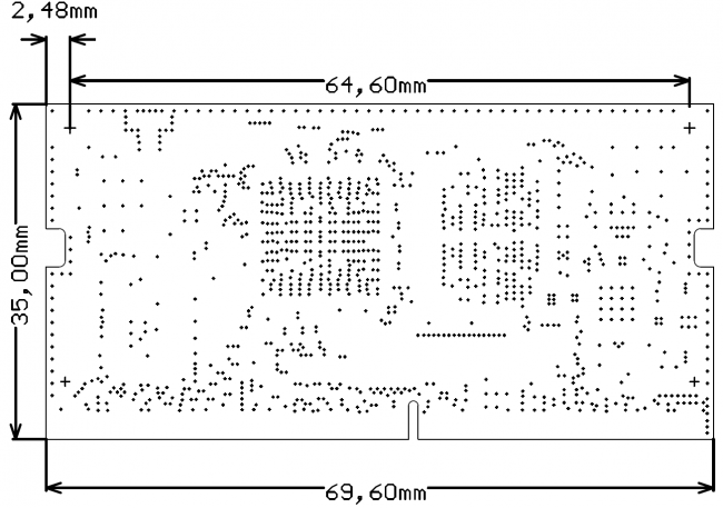
Dimensions
