StarCB-6ULL-STD Datasheet and Pinout
From SomLabs Wiki

StarCB-6ULL-STD Datasheet and Pinout
Contents
- 1 General description
- 2 Features
- 3 Pictures of StarCB-6LLL-STD board
- 4 Ordering info
- 5 Block Diagram
- 6 Electrical parameters
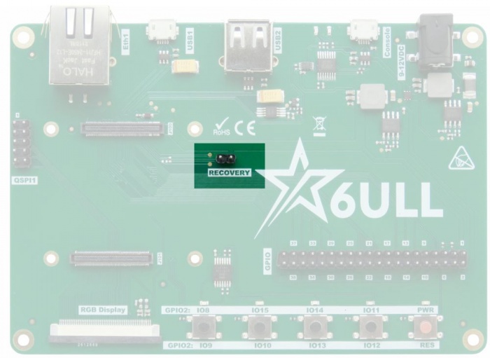
- 7 Recovery jumper (J501, 2.54mm)
- 8 USB interfaces (J200 and J201)
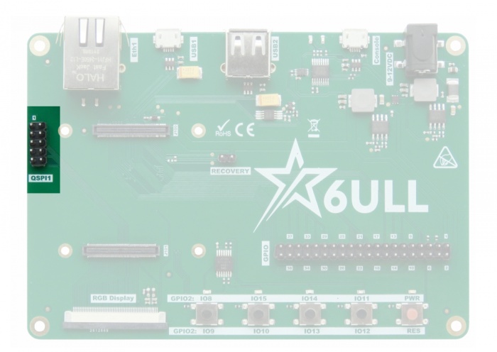
- 9 QSPI interface (J502, 2x5 gold-pin, 2.54mm)
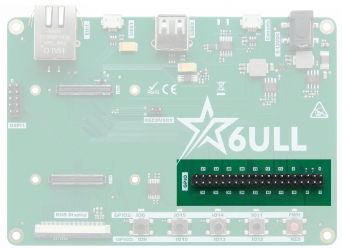
- 10 GPIO connector (J500, 2x20 gold-pin, 2.54mm)
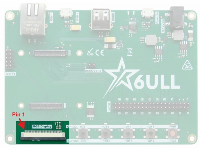
- 11 Display interface (J300, FPC/FFC 0.5mm)
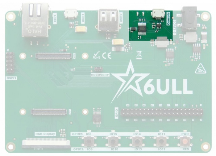
- 12 USB Console Port
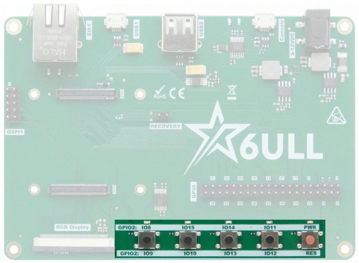
- 13 User Interface (switches and LEDs)
- 14 Dimensions
General description
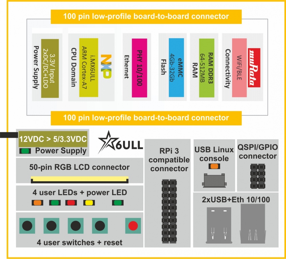
StarCB-6ULL-STD is a carrier board for the StarSOM-6ULL family of computer-on-modules, which are powered by NXP i.MX 6ULL application processors (ARM Cortex-A7). A carrier board, together with a System on Module (SoM), makes a complete development platform similar to SBC. The carrier board houses the most common interfaces such as USB, Ethernet, etc. A large variety of interfaces allows to use it as both a complete development platform or as a stand-alone end-product.
The carrier board connects with the SoM via a board-to-board, low profile connectors.
Applications
- IoT Sensor Hubs
- Home Appliances
- IoT gateways
- Protocol converters
- Home Automation – Smart Home
- Point-of-sales (POS) terminals
- Cash Register
- 2D barcode scanners and printers
- Smart grid infrastructure
- Residential gateways
- Outdoor equipment
Features
- Carrier Board (Base Board) compatible with the StarSOM-6ULL family of modules based iMX6ULL application processors
- SoM Interface: 2x100 board-to-board connectors
- Debug Interface: Linux console (vCOM/USB)
- Expansion Connectors:
- QSPI connector 2x10 Pin Header (Male)
- GPIO connector 2x20 Pin Header (Male)
- Communication Connectors:
- 1x Ethernet 10/100Mbit/s, RJ45
- 1x USB Host Type A connectors
- 1x USB OTG Micro AB connector
- 1x Console MicroUSB B connector
- Display Interface:
- 50-pin FFC/FPC parallel RGB (up to 24 bits)
- User Interface:
- 4+1 Pushbuttons
- 4+3 LEDs
- External Power Supply 9-12V DC
- Temperature Range: 0 to +70°C
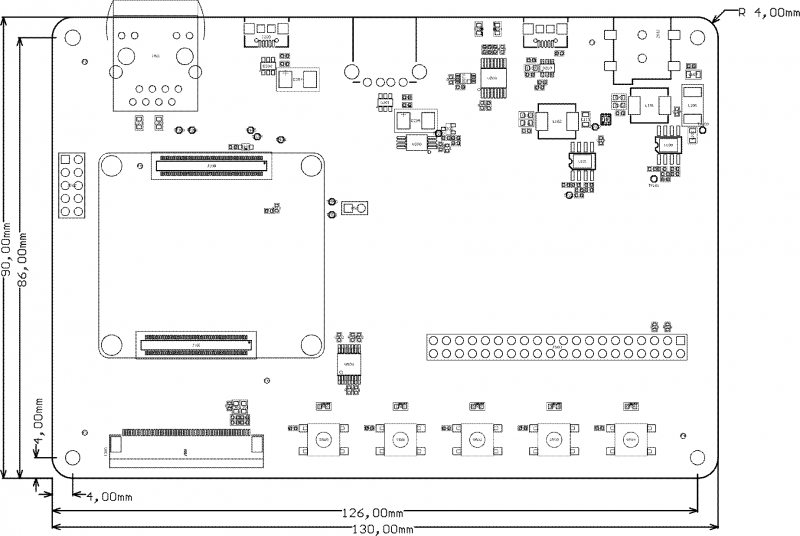
- Board Size: 130mm x 90mm x 20mm
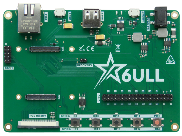
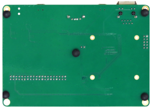
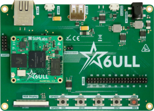
Pictures of StarCB-6LLL-STD board
| Version | Photo |
|---|---|
| StarCB-6LL-STD board only | |
| StarCB-6LL-STD board - bottom side | |
| StarCB-6LL-STD board with StarSOM-6ULL installed |
Ordering info
Block Diagram
Electrical parameters
| Parameter | Value | Units | Comment | ||
|---|---|---|---|---|---|
| Min. | Typ. | Max. | |||
| Power Supply | 9.0 | 12.0 | 15.0 | V | Positive pole on central connector of J400 |
| Supply current | - | - | 0.09 | A | Excluding SOM, LCD, USB and antoher external loads |
| GPIO voltage | 3.3 | V | |||
Recovery jumper (J501, 2.54mm)
| Pin | Signal | Description |
|---|---|---|
| 1 | Recovery | SOM recovery input |
| 2 | GND |
Note:
1. To start recovery procedure connect pins 1 and 2 of J501 and press RES (red) button.
USB interfaces (J200 and J201)
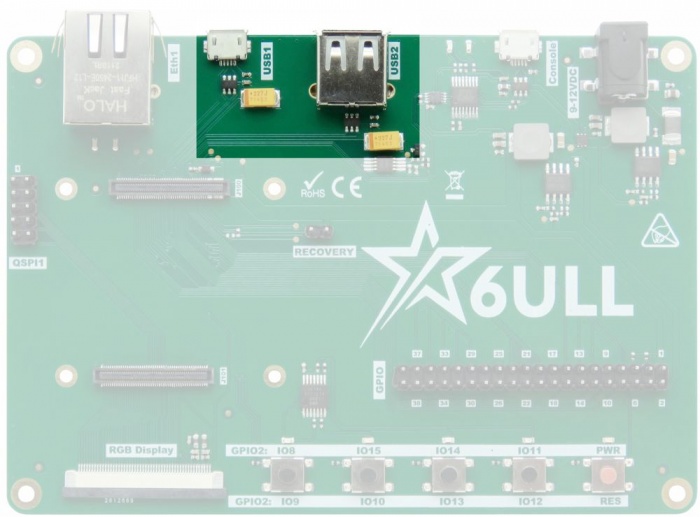
1. Connector J200 (5-pin MicroUSB-OTG) is connected to USB1 MPU transceiver.
2. USB1 is OTG type interface used for application and recovery purposes.
3. Connector J201 (4-pin USB-A) is connected to USB2 MPU transceiver.
4. USB1-ID (OTG identification line) is connected to GPIO1.00 of MPU.
5. USB1-VBUS-EN (USB device power supply enable line) is connected to GPIO1.05 of MPU.
QSPI interface (J502, 2x5 gold-pin, 2.54mm)
| Pin | Signal | Description |
|---|---|---|
| 1 | QSPI1.D0 | optionally GPIO4.12 |
| 2 | VDD-EMMC | Internal (on SOM) 1.8V LDO output as reference or power supply voltage for QSPI (SDIO) interface |
| 3 | QSPI1.D1 | optionally GPIO4.13 |
| 4 | QSPI1.CLK | optionally GPIO4.11 |
| 5 | QSPI1.D2 | optionally GPIO4.14 |
| 6 | QSPI1.CS0 | optionally GPIO4.16 |
| 7 | QSPI1.D3 | optionally GPIO4.15 |
| 8 | - | - |
| 9 | QSPI1.DQS | optionally GPIO4.10 |
| 10 | GND | - |
GPIO connector (J500, 2x20 gold-pin, 2.54mm)
| Pin | Signal | Description |
|---|---|---|
| 1 | VDD-3V3 | Power supply for external loads (up to 300 mA) |
| 2 | VDD-5V0 | Power supply for external loads (up to 200 mA) |
| 3 | I2C2-SDA | 4.7k pull-up resistor connected Connected to LCD J300 connector (touch panel controller) Optionally GPIO1.31 |
| 4 | VDD-5V0 | Power supply for external loads (up to 200 mA) |
| 5 | I2C2-SCL | 4.7k pull-up resistor connected Connected to LCD J300 connector (touch panel controller) Optionally GPIO1.30 |
| 6 | GND | - |
| 7 | TAMPER.0 | optionally GPIO5.00 |
| 8 | UART3.TXD | optionally GPIO1.24 |
| 9 | GND | - |
| 10 | UART3.RXD | optionally GPIO1.25 |
| 11 | TAMPER.1 | optionally GPIO5.01 |
| 12 | UART3.RTS | optionally GPIO1.27 |
| 13 | TAMPER.2 | optionally GPIO5.02 |
| 14 | GND | - |
| 15 | TAMPER.3 | optionally GPIO5.03 |
| 16 | UART3.CTS | optionally GPIO1.26 |
| 17 | VDD-3V3 | Power supply for external loads (up to 300 mA) |
| 18 | JTAG.TDI | optionally GPIO1.13 |
| 19 | UART1.CTS | optionally GPIO1.18 |
| 20 | GND | - |
| 21 | UART1.RTS | optionally GPIO1.19 |
| 22 | JTAG.TMS | optionally GPIO1.11 |
| 23 | UART1.RXD | optionally GPIO1.17 |
| 24 | UART1.TXD | optionally GPIO1.16 |
| 25 | GND | - |
| 26 | TAMPER.9 | optionally GPIO5.09 |
| 27 | - | - |
| 28 | - | - |
| 29 | TAMPER.4 | optionally GPIO5.04 |
| 30 | GND | - |
| 31 | UART2.RXD | optionally GPIO1.21 |
| 32 | TAMPER.8 | optionally GPIO5.08 |
| 33 | UART2.TXD | optionally GPIO1.20 |
| 34 | GND | - |
| 35 | UART2.RTS | optionally GPIO1.23 |
| 36 | TAMPER.7 | optionally GPIO5.07 |
| 37 | UART2.CTS | optionally GPIO1.22 |
| 38 | TAMPER.6 | optionally GPIO5.06 |
| 39 | GND | - |
| 40 | TAMPER.5 | optionally GPIO5.05 |
Display interface (J300, FPC/FFC 0.5mm)
| Pin | Signal | Description |
|---|---|---|
| 1 | LCD.DATA00 | B0 |
| 2 | LCD.DATA01 | B1 |
| 3 | LCD.DATA02 | B2 |
| 4 | LCD.DATA03 | B3 |
| 5 | LCD.DATA04 | B4 |
| 6 | LCD.DATA05 | B5 |
| 7 | LCD.DATA06 | B6 |
| 8 | LCD.DATA07 | B7 |
| 9 | GND | - |
| 10 | LCD.DATA08 | G0 |
| 11 | LCD.DATA09 | G1 |
| 12 | LCD.DATA10 | G2 |
| 13 | LCD.DATA11 | G3 |
| 14 | LCD.DATA12 | G4 |
| 15 | LCD.DATA13 | G5 |
| 16 | LCD.DATA14 | G6 |
| 17 | LCD.DATA15 | G7 |
| 18 | GND | - |
| 19 | LCD.DATA16 | R0 |
| 20 | LCD.DATA17 | R1 |
| 21 | LCD.DATA18 | R2 |
| 22 | LCD.DATA19 | R3 |
| 23 | LCD.DATA20 | R4 |
| 24 | LCD.DATA21 | R5 |
| 25 | LCD.DATA22 | R6 |
| 26 | LCD.DATA23 | R7 |
| 27 | GND | - |
| 28 | LCD.ENABLE | - |
| 29 | LCD.HSYNC | - |
| 30 | LCD.VSYNC | - |
| 31 | GND | - |
| 32 | LCD.CLK | - |
| 33 | GND | - |
| 34 | GPIO1.04 | TS-YPUL |
| 35 | GPIO1.03 | TS-YNUR |
| 36 | GPIO1.02 | TS-YPLL |
| 37 | GPIO1.01 | TS-YNLR |
| 38 | - | - |
| 39 | - | - |
| 40 | - | - |
| 41 | - | - |
| 42 | I2C2-SCL | 4.7k pull-up resistor connected Touch panel controller interface |
| 43 | I2C2-SDA | 4.7k pull-up resistor connected Touch panel controller interface |
| 44 | GND | - |
| 45 | VDD-3V3 | +3.3V power source fr LCD module |
| 46 | VDD-3V3 | +3.3V power source fr LCD module |
| 47 | VDD-3V3 | +3.3V power source fr LCD module |
| 48 | VDD-3V3 | +3.3V power source fr LCD module |
| 49 | LCD.RESET | Optional reset signal GPIO3.04 |
| 50 | PWREN | Optional power-enable signal GPIO1.15 |
USB Console Port
| MPU Port | GPIO | Description |
|---|---|---|
| CONSOLE-TXD | UART4.TXD | TxD line from MPU to vCOM |
| CONSOLE-RXD | UART4.RXD | RxD line to MPU from vCOM |
Note:
1. Linux console port (UART4 in MPU) uses vCOM interface.
2. Two LEDs near MicroUSB connectors allow to monitor connection to USB interface and data transmission.
User Interface (switches and LEDs)
User switches
| Switch | GPIO | Description |
|---|---|---|
| S500 (black, most on the left) | GPIO2.09 | Optionally ENET2.RXD1 |
| S501 | GPIO2.10 | Optionally ENET2.RXEN |
| S502 | GPIO2.13 | Optionally ENET2.TXEN |
| S503 (black, on the right) | GPIO2.12 | Optionally ENET2.TXD1 |
System switches
| Switch | Signal name | Description |
|---|---|---|
| S504 (on the right, red) | Reset | Connected to POR input on SOM |
User LEDs
| LED | GPIO | Description |
|---|---|---|
| D500 (most on the left) | GPIO2.08 | User LED buffered with inverter Optionally ENET2.RXD0 |
| D501 | GPIO2.15 | User LED buffered with inverter Optionally ENET2.RXER |
| D502 | GPIO2.14 | User LED buffered with inverter Optionally ENET2.TXCLK |
| D503 (most on the right) | GPIO2.11 | User LED buffered with inverter Optionally ENET2.TXD0 |
System LEDs
| LED | GPIO | Description |
|---|---|---|
| D504 | Power | Power active (3.3V) |

