VisionCB-STM32MP1-STD Datasheet and Pinout
From SomLabs Wiki

VisionCB-STM32MP1-STD v.1.1 Datasheet and Pinout
Contents
- 1 General description
- 2 Features
- 3 Pictures of VisionCB-STM32MP1-STD v1.1 board
- 4 Ordering info
- 5 Block Diagram
- 6 Electrical parameters
- 7 Boot Selector
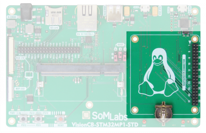
- 8 Raspberry Pi compatible I/O header
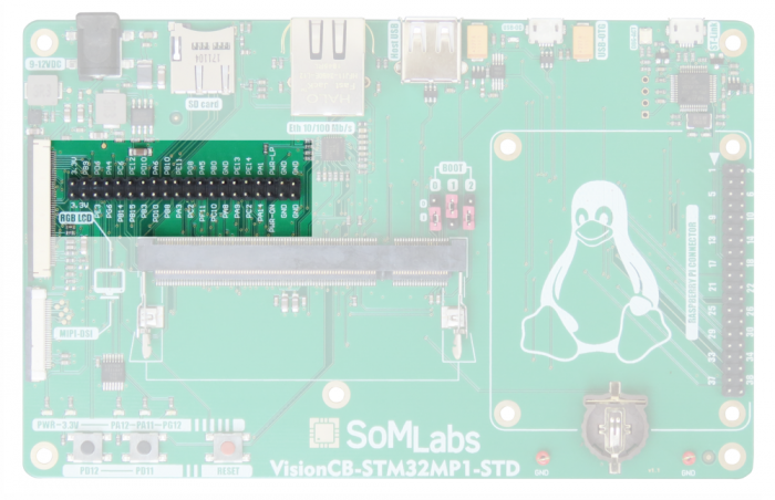
- 9 Universal I/O header
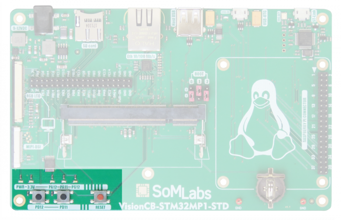
- 10 User Interface (switches and LEDs)
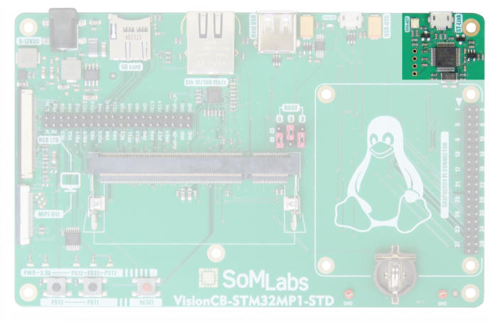
- 11 Console Port
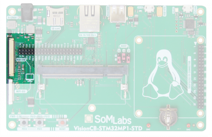
- 12 LCD Parallel Connector
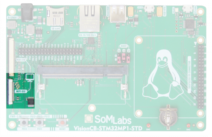
- 13 LCD MIPI-CSI Connector
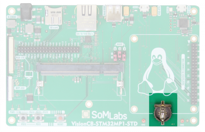
- 14 MPU internal RTC Battery Socket
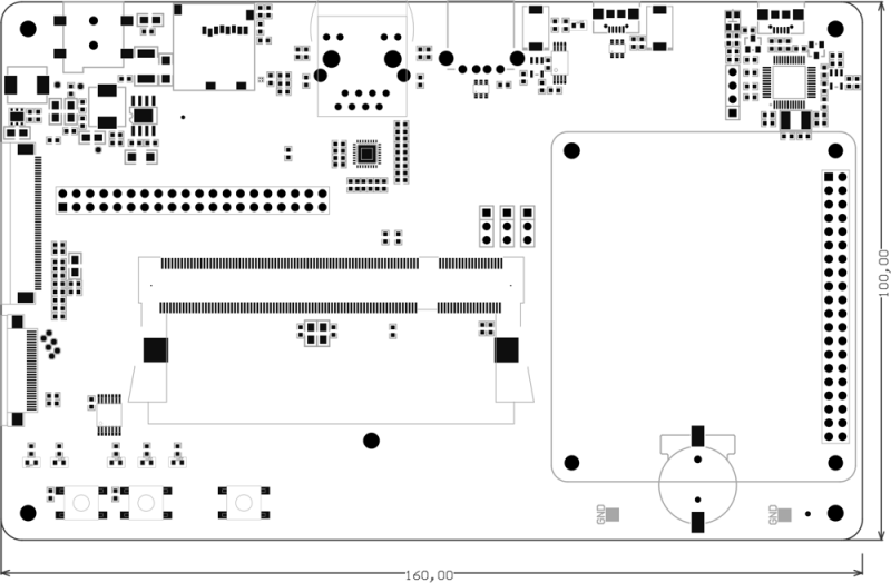
- 15 Dimensions
General description
VisionCB-STM32MP1-STD is a carrier board for the VisionSOM-STM32MP1 family of computer-on-modules which are powered by STMicroelectronics STM32MP15x application processors (single or dual core ARM Cortex-A7 + internal microcontroller Cortex-M4). A carrier board, together with a System on Module (SoM), makes a complete development platform similar to SBC. The carrier board houses the most common interfaces such as debugger, USB, Ethernet, UART, etc. A large variety of interfaces allows to use it as both a complete development platform or as a stand-alone end-product.
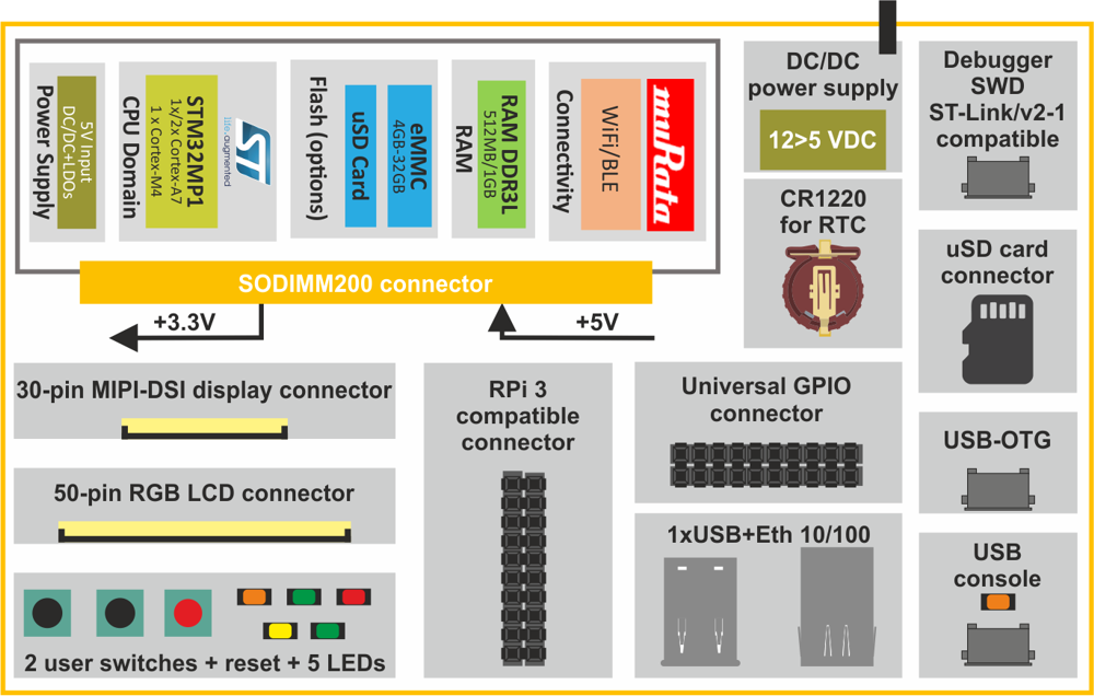
The carrier board connects with the SoM via a standard SODIMM200 connector. VisionCB-STM32MP1-STD is equippped with internal ST-Link/v2-1 debugger with SWD interface and serial USB console port.
Applications
- Industrial embedded Linux computer
- Home Appliances
- Home Automation – Smart Home
- Human-machine Interfaces (HMI)
- Point-of-sales (POS) terminals
- Cash Register
- 2D barcode scanners and printers
- Smart grid Infrastructure
- IoT gateways
- Residential getaways
- Machine vision equipment
- Robotics
- Fitness/outdoor equipment
Features
- Carrier Board (Base Board) compatible with the VisionSOM-STM32MP1 family of modules based on STMicroelectronics STM32MP15x application processors
- SoM Interface: SODIMM200
- Debug Interface: built-in ST-Link/v2-1 SWD debugger
- Expansion Connectors:
- Raspberry Pi compatible connectors 2x20 Pin Header (Male)
- Universal 2x20 Pin Header (Male)
- MicroSD card socket
- Communication Connectors:
- 1x Ethernet 10/100Mbit/s, RJ45
- 1x USB Host Type A connectors
- 1x USB OTG Micro AB connector
- 1x Console MicroUSB B connector
- Display Interface:
- 50-pin FFC/FPC Parallel RGB – 24-bit
- 30-pin FFC/FPC MIPI-DSI
- User Interface:
- 3 Pushbuttons
- 5 LEDs
- Boot selector
- External Power Supply 9-12V DC
- Temperature Range: 0 to +70°C
- Board Size: 160mm x 100mm x 17mm
Pictures of VisionCB-STM32MP1-STD v1.1 board
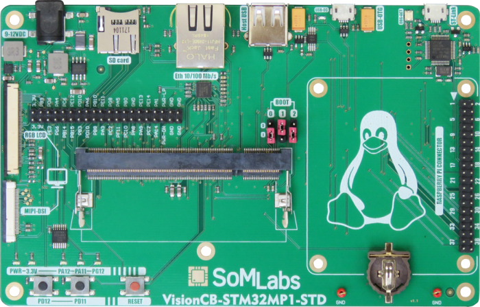
| Version | Photo |
|---|---|
| VisionCB-STM32MP1-STD v1.1 board only |
Ordering info
Block Diagram
Electrical parameters
| Parameter | Value | Units | Comment | ||
|---|---|---|---|---|---|
| Min. | Typ. | Max. | |||
| Power Supply | 9.0 | 12.0 | 15.0 | V | Positive pole on central connector of J102 |
| Supply current | - | - | 0.15 | A | Excluding LCD, USB and antoher external loads |
| LCD Power Supply | 3.25 | 3.4 | 3.5 | V | Optionally 5V |
| MicroSD Card Power Supply | 3.15 | 3.3 | 3.45 | V | - |
| GPIO voltage | 3.3 | V | - | ||
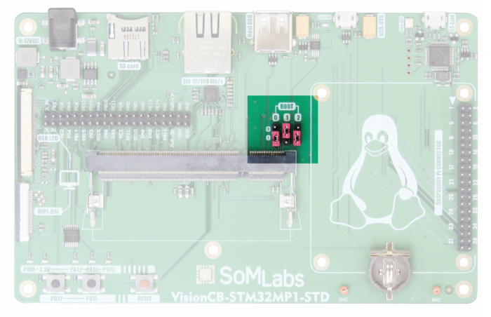
Boot Selector
| BOOTx | Boot Mode | Description | ||
|---|---|---|---|---|
| BOOT2 | BOOT1 | BOOT0 | ||
| 0 | 0 | 0 | UART and USB | Wait incoming connection on: - USART2/3/6 and UART4/5/7/8 on default pins - USB high-speed device |
| 0 | 0 | 1 | Serial NOR Flash | Not used on VisionSOM-STM32MP1 |
| 0 | 1 | 0 | eMMC | eMMC on SDMMC2 |
| 0 | 1 | 1 | NAND Flash | Not used on VisionSOM-STM32MP1 |
| 1 | 0 | 0 | - | Not used on VisionSOM-STM32MP1 |
| 1 | 0 | 1 | SD card | SD card on SDMMC1 |
| 1 | 1 | 0 | UART and USB | Wait incoming connection on: - USART2/3/6 and UART4/5/7/8 on default pins - USB high-speed device on OTG_HS_DP/DM pins |
| 1 | 1 | 1 | Serial NAND Flash | Not used on VisionSOM-STM32MP1 |
By default BOOT2...BOOT0 lines are pulled-down with 1k resistors
Raspberry Pi compatible I/O header
| Pin | Default function name | Description |
|---|---|---|
| 1 | +3.3V | +3.3V generated by DC/DC built-in SOM (limited current load) |
| 2 | +5V | +5V generated by carrier board built-in DC/DC converter |
| 3 | DSI-I2C-SDA | I2C4 SDA line |
| 4 | +5V | +5V generated by carrier board built-in DC/DC converter |
| 5 | DSI-I2C-SCL | I2C4 SCL line |
| 6 | GND | - |
| 7 | UART8-CTS | Default: UART8 CTS line or universal GPIO with 3.3V logic levels |
| 8 | UART3-TXD | Default: UART3 TXD line or universal GPIO with 3.3V logic levels |
| 9 | GND | - |
| 10 | UART3-RXD | Default: UART3 RXD line or universal GPIO with 3.3V logic levels |
| 11 | UART8-RTS | Default: UART8 RTS line or universal GPIO with 3.3V logic levels |
| 12 | GPIO-PD12 | Shared with switch S100/10k pullup |
| 13 | - | - |
| 14 | GND | - |
| 15 | - | - |
| 16 | GPIO-PD11 | Shared with switch S101/10k pullup |
| 17 | +3.3V | +3.3V generated by DC/DC built-in SOM (limited current load) |
| 18 | GPIO-PG12 | Shared with user LED (D102, yellow) LED is buffered by logic inverter |
| 19 | LCD-R6 (DATA22) | PA8 GPIO line SPI3 MOSI |
| 20 | GND | - |
| 21 | LCD-B3 (DATA3) | PD10 GPIO line SPI3 MISO |
| 22 | GPIO-PA12 | Shared with user LED (D100, green) LED is buffered by logic inverter |
| 23 | LCD-R2 (DATA18) | PC10 GPIO line SPI3 SCK |
| 24 | GPIO-PA11 | Shared with user LED (D101, red) LED is buffered by logic inverter |
| 25 | GND | - |
| 26 | USART6-RXD | Default: UART6 RXD line or universal GPIO with 3.3V logic levels |
| 27 | - | - |
| 28 | - | - |
| 29 | DSI-BL-PWM | PD15 GPIO line TIM4 CH4 PWM output |
| 30 | GND | - |
| 31 | GPIO-PB1-ADC1-5 | Universal GPIO line with 3.3V logic levels or ADC input |
| 32 | USART6-TXD | Default: UART6 TXD line or universal GPIO with 3.3V logic levels |
| 33 | GPIO-PC0-ADC1-10 | Universal GPIO line with 3.3V logic levels or ADC input |
| 34 | GND | - |
| 35 | GPIO-PC3-ADC1-13 | Universal GPIO line with 3.3V logic levels or ADC input |
| 36 | GPIO-PA13 | Shared with PHY Ethernet controller interrupt line |
| 37 | GPIO-PA0-ADC1-16 | Universal GPIO line with 3.3V logic levels or ADC input |
| 38 | GPIO-PB6 | Universal GPIO with 3.3V logic levels |
| 39 | GND | - |
| 40 | GPIO-PF10 | Universal GPIO with 3.3V logic levels |
Universal I/O header
| Pin | Default function name | Description |
|---|---|---|
| 1 | +3.3V | +3.3V generated by DC/DC built-in SOM (limited current load) |
| 2 | +3.3V | +3.3V generated by DC/DC built-in SOM (limited current load) |
| 3 | +3.3V | +3.3V generated by DC/DC built-in SOM (limited current load) |
| 4 | LCD-B7 (DATA7) | PB9 - universal GPIO with 3.3V logic levels |
| 5 | SD2-CLK | PE3 - universal GPIO with 3.3V logic levels |
| 6 | LCD-B2 (DATA2) | PD6 - universal GPIO with 3.3V logic levels |
| 7 | SD2-CMD | PG6 - universal GPIO with 3.3V logic levels |
| 8 | LCD-VSYNC | PA4 - universal GPIO with 3.3V logic levels |
| 9 | SD2-DATA0 | PB14 - universal GPIO with 3.3V logic levels |
| 10 | LCD-HSYNC | PC6 - universal GPIO with 3.3V logic levels |
| 11 | SD2-DATA1 | PB15 - universal GPIO with 3.3V logic levels |
| 12 | LCD-B4 (DATA4) | PE12 - universal GPIO with 3.3V logic levels |
| 13 | SD2-DATA2 | PB3 - universal GPIO with 3.3V logic levels |
| 14 | LCD-B3 (DATA3) | PD10 - universal GPIO with 3.3V logic levels MISO line of SPI3 |
| 15 | SD2-DATA3 | PB4 - universal GPIO with 3.3V logic levels
On the carrier board 1.1 incorrectly marked as PD10 |
| 16 | LCD-G2 (DATA10) | PA6 - universal GPIO with 3.3V logic levels |
| 17 | LCD-B6 (DATA6) | PB8 - universal GPIO with 3.3V logic levels |
| 18 | LCD-G4 (DATA12) | PB10 - universal GPIO with 3.3V logic levels |
| 19 | LCD-B5 (DATA5) | PA3 - universal GPIO with 3.3V logic levels |
| 20 | LCD-G3 (DATA11) | PE11 - universal GPIO with 3.3V logic levels |
| 21 | LCD-G6 (DATA14) | PC7 - universal GPIO with 3.3V logic levels
On the carrier board 1.1 incorrectly marked as PC2 |
| 22 | LCD-G7 (DATA15) | PG8 - universal GPIO with 3.3V logic levels |
| 23 | LCD-G5 (DATA13) | PF11 - universal GPIO with 3.3V logic levels |
| 24 | LCD-R4 (DATA20) | PA5 - universal GPIO with 3.3V logic levels |
| 25 | LCD-R2 (DATA18) | PC10 - universal GPIO with 3.3V logic levels SCK line of SPI3 |
| 26 | LCD-R3 (DATA19) | PB0 - universal GPIO with 3.3V logic levels |
| 27 | LCD-R6 (DATA22) | PA8 - universal GPIO with 3.3V logic levels MOSI line of SPI3 |
| 28 | LCD-R7 (DATA23) | PE15 - universal GPIO with 3.3V logic levels
On the carrier board 1.1 incorrectly marked as GND |
| 29 | LCD-R5 (DATA21) | PA9 - universal GPIO with 3.3V logic levels |
| 30 | LCD-DE | PE13 - universal GPIO with 3.3V logic levels |
| 31 | GPIO-PC2 | PC2 - universal GPIO with 3.3V logic levels |
| 32 | LCD-PCLK | PE14 - universal GPIO with 3.3V logic levels |
| 33 | GPIO-PA14 | PA14 - universal GPIO with 3.3V logic levels |
| 34 | LCD-RESET/DSI-RESET | PA1 - universal GPIO with 3.3V logic levels |
| 35 | PWR-ON | Function depends on LPCFG configuration (output) |
| 36 | PWR-LP | Low power mode signalling output |
| 37 | GND | - |
| 38 | GND | - |
| 39 | GND | - |
| 40 | GND | - |
User Interface (switches and LEDs)
User switches
| Switch | GPIO | Description |
|---|---|---|
| S100 (left) | PD12 | 10k pull-up |
| S101 (right) | PD11 | 10k pull-up |
User LEDs
| LED | GPIO | Description |
|---|---|---|
| D100 | PA12 | LED is buffered by logic inverter |
| D101 | PA11 | LED is buffered by logic inverter |
| D102 | PG12 | LED is buffered by logic inverter |
Console Port
Linux console port uses vCOM interface provided by ST-Link/v2-1.
| MPU Port | GPIO | Description |
|---|---|---|
| UART4-TXD | PG11 | - |
| UART4-RXD | PB2 | - |
LCD Parallel Connector
| Pin | Default function name | Description |
|---|---|---|
| 1 | LCD-B0 (DATA0) | Internally connected to GND |
| 2 | LCD-B1 (DATA1) | Internally connected to GND |
| 3 | LCD-B2 (DATA2) | Connected to PD6 |
| 4 | LCD-B3 (DATA3) | Connected to PD10 |
| 5 | LCD-B4 (DATA4) | Connected to PE12 |
| 6 | LCD-B5 (DATA5) | Connected to PA3 |
| 7 | LCD-B6 (DATA6) | Connected to PB8 |
| 8 | LCD-B7 (DATA7) | Connected to PB9 |
| 9 | GND | - |
| 10 | LCD-G0 (DATA8) | Internally connected to GND |
| 11 | LCD-G1 (DATA9) | Internally connected to GND |
| 12 | LCD-G2 (DATA10) | Connected to PA6 |
| 13 | LCD-G3 (DATA11) | Connected to PE11 |
| 14 | LCD-G4 (DATA12) | Connected to PB10 |
| 15 | LCD-G5 (DATA13) | Connected to PF11 |
| 16 | LCD-G6 (DATA14) | Connected to PC7 |
| 17 | LCD-G7 (DATA15) | Connected to PG8 |
| 18 | GND | - |
| 19 | LCD-R0 (DATA16) | Internally connected to GND |
| 20 | LCD-R1 (DATA17) | Internally connected to GND |
| 21 | LCD-R2 (DATA18) | Connected to PC10 |
| 22 | LCD-R3 (DATA19) | Connected to PB0 |
| 23 | LCD-R4 (DATA20) | Connected to PA5 |
| 24 | LCD-R5 (DATA21) | Connected to PA9 |
| 25 | LCD-R6 (DATA22) | Connected to PA8 |
| 26 | LCD-R7 (DATA23) | Connected to PE15 |
| 27 | GND | - |
| 28 | LCD-DE | Connected to PE13 |
| 29 | LCD-HSYNC | Connected to PC6 |
| 30 | LCD-VSYNC | Connected to PA4 |
| 31 | GND | - |
| 32 | LCD-PCLK | Connected to PE14 |
| 33 | GND | - |
| 34 | - | - |
| 35 | - | - |
| 36 | TP-INT | Connected to PA14 line 4,7k pull-up |
| 37 | PWM | Connected to PD15 line PWM backlight brightness adjustment Channel 4 of TIM4 (PWM) |
| 38 | - | - |
| 39 | - | - |
| 40 | - | - |
| 41 | - | - |
| 42 | I2C4_SCL | Connected to PE2 line 4,7k pull-up |
| 43 | I2C4_SDA | Connected to PB7 line 4,7k pull-up |
| 44 | GND | |
| 45 | +3.3V | LCD logic power supply |
| 46 | +3.3V | LCD logic power supply |
| 47 | +3.3V | LCD backlight power supply |
| 48 | +3.3V | LCD backlight power supply |
| 49 | LCD-RESET | Connected to PA1 line |
| 50 | BACKLT PWR EN | Connected to PC2 line Backlight ON/OFF 4,7k pull-up |
Note: Simultaneous use of both displays (MIPI-DSI and Parallel) is not possible
LCD MIPI-CSI Connector
| Pin | Default function name | Description |
|---|---|---|
| 1 | GND | - |
| 2 | DSI-CKp | Positive MIPI clock signal |
| 3 | DSI-CKn | Negative MIPI clock signal |
| 4 | GND | - |
| 5 | DSI-D0p | Positive Lane 0 signal |
| 6 | DSI-D0n | Negative Lane 0 signal |
| 7 | GND | - |
| 8 | DSI-D1p | Positive Lane 1 signal |
| 9 | DSI-D1n | Negative Lane 1 signal |
| 10 | GND | - |
| 11 | - | - |
| 12 | - | - |
| 13 | GND | - |
| 14 | - | - |
| 15 | - | - |
| 16 | GND | - |
| 17 | DSI-I2C-SCL | Connected to PE2 line 4,7k pull-up |
| 18 | DSI-I2C-SDA | Connected to PB7 line 4,7k pull-up |
| 19 | GND | - |
| 20 | DSI-RESET | Connected to PA1 line |
| 21 | DSI-TP-INT | Connected to PA14 line |
| 22 | DSI-TP-RST | - |
| 23 | GND | - |
| 24 | +3.3V | LCD logic power supply |
| 25 | +3.3V | LCD logic power supply |
| 26 | +5V | LCD backlight power supply |
| 27 | +5V | LCD backlight power supply |
| 28 | DSI-BL-PWM | Connected to PD15 line PWM backlight brightness adjustment Channel 4 of TIM4 (PWM) |
| 29 | DSI-BL-EN | Connected to PC2 line Backlight ON/OFF 4,7k pull-up |
| 30 | GND | - |
Note: Simultaneous use of both displays (MIPI-DSI and Parallel) is not possible
MPU internal RTC Battery Socket
Optional CR1220 lithium 3V battery is connected to VDD-COIN-3V RTC backup line.
It is not allowed to use a primary battery, because of a small reverse charging current.

