Difference between revisions of "SL-MIPI-LVDS-HDMI-CNV-11 Datasheet and Pinout"
From SomLabs Wiki
(Created page with "{{PageHeader|Display module SL-TFT7-TP-800-480 Datasheet and Pinout}} __toc__ __jzpdf__ == General description == 800px|center <br>...") |
(→General description) |
||
| (45 intermediate revisions by the same user not shown) | |||
| Line 1: | Line 1: | ||
| − | {{PageHeader| | + | {{PageHeader|SL-MIPI-LVDS-HDMI-CNV MIPI-DSI to LVDS and HDMI converter Datasheet and Pinout}} __toc__ |
__jzpdf__ | __jzpdf__ | ||
== General description == | == General description == | ||
| − | [[File: | + | [[File:sl-mipi-lvds-hdmi-cnv-v11.jpg|800px|center]] |
<br> | <br> | ||
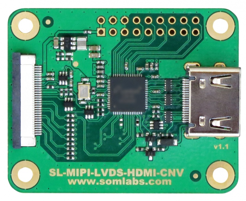
| − | SL- | + | SL-MIPI-LVDS-HDMI-CNV (MIPI-DSI to LVDS HDMI converter) is flexible MIPI-DSI to LVDS and/or HDMI converter. The solution we dedicate to SoMLabs carrier boards equipped with MIPI-DSI interface (with FPC30 connector). Converter is fully compliant with DSI1.02 and HDMI1.4 and converts video stream up to 1080p @60Hz/8b. |
| − | + | SL-MIPI-LVDS-HDMI-CNV is fully compatible with SoMLabs carrier borads equipeed with MIPI-DSI FPC30 connector. | |
== Features == | == Features == | ||
| − | * | + | * MIPI-DSI to LVDS and/or HDMI display converter |
| − | * | + | * Integrated D-PHY1.1 (DSI1.02) |
| − | * | + | * From 1 up to 4 MIPI input data lanes |
| − | * | + | * Compatible with MIPI-DSI data packets: 18bpp, RGB666 and 24bpp RGB888 |
| − | * | + | * Input bandwidth up tp 6Gb/s (4 lanes) |
| − | + | * LVDS output clocking up to 154 MHz | |
| − | * | + | * Fully compatible with SoMLabs carrier board: |
| − | * | + | ** VisionCB-8M-STD (dedicated to i.MX8M mini multicore MPU) |
| − | ** VisionCB-STD | + | ** VisionCB-STM32MP1-STD (dedicated to STM32MP1 multicore MPU) |
| − | ** VisionCB-STD | + | * Plug & Play solution for SoMLabs customers |
| − | + | * Integrated stereo audio channel | |
| − | + | * Connection with carrier board using FPC30 cable A-A type | |
| − | |||
| − | |||
| − | |||
| − | |||
| − | |||
| − | |||
== Pictures == | == Pictures == | ||
| − | [[File: | + | [[File:sl-mipi-lvds-hdmi-cnv-v11-angle-OK.jpg|800px|center]]<br> |
| − | [[File: | + | [[File:sl-mipi-lvds-hdmi-cnv-v11-CB1.jpg|800px|center]]<br> |
| − | [[File: | + | [[File:sl-mipi-lvds-hdmi-cnv-v11-CB2.jpg|800px|center]]<br> |
| − | [[File: | + | [[File:sl-mipi-lvds-hdmi-cnv-v11.jpg|800px|center]]<br> |
== Ordering info == | == Ordering info == | ||
| − | '''SL- | + | '''SL-MIPI-LVDS-HDMI-CNV''' - FPC 30-pin flat cable (A-A) is included. |
== Operating ranges == | == Operating ranges == | ||
| Line 44: | Line 38: | ||
|- | |- | ||
| Power Supply | | Power Supply | ||
| − | | <center>5.0</center> | + | | <center>3.3 & 5.0</center> |
| <center>V</center> | | <center>V</center> | ||
| − | | | + | | Powered from carrier board |
|- | |- | ||
| Current | | Current | ||
| − | | <center>0. | + | | <center>0.1</center> |
| <center>A</center> | | <center>A</center> | ||
| − | | Maximum value | + | | Maximum peak value |
| − | |||
| − | |||
| − | |||
| − | |||
| − | |||
| − | |||
| − | |||
| − | |||
| − | |||
| − | |||
|- | |- | ||
|Environment temperature | |Environment temperature | ||
| − | |<center>- | + | |<center>-40…+85</center> |
|<sup>o</sup>C | |<sup>o</sup>C | ||
| - | | - | ||
| Line 82: | Line 66: | ||
| +5V | | +5V | ||
| Supply Voltage | | Supply Voltage | ||
| − | | 4. | + | | 4.75 |
| 5.0 | | 5.0 | ||
| − | | 5. | + | | 5.25 |
| V | | V | ||
|- | |- | ||
| − | | - | + | | +3.3V |
| − | | | + | | Supply Voltage |
| − | | | + | | 3.2 |
| − | | | + | | 3.3 |
| − | | | + | | 3.35 |
| + | | V | ||
| + | |- | ||
| + | | I<sub>5V</sub> | ||
| + | | Supply Current (5V) | ||
| + | | 40 | ||
| + | | 80 | ||
| + | | 100 | ||
| + | | mA | ||
| + | |- | ||
| + | | I<sub>3.3V</sub> | ||
| + | | Supply Current (3.3V) | ||
| + | | 1 | ||
| + | | 2.2 | ||
| + | | 8 | ||
| mA | | mA | ||
|- | |- | ||
| − | | VIO | + | | VIO<sub>I2C</sub> |
| − | | | + | | I2C Input Voltage |
| 0 | | 0 | ||
| 3.3 | | 3.3 | ||
| Line 101: | Line 99: | ||
| V | | V | ||
|- | |- | ||
| − | | | + | | VIO<sub>RES/SPDIF</sub> |
| − | | | + | | RES/SPDIF Input Voltage |
| 0 | | 0 | ||
| 3.3 | | 3.3 | ||
| Line 108: | Line 106: | ||
| V | | V | ||
|- | |- | ||
| − | + | | f<sub>I2C</sub> | |
| − | + | | I2C Controller Speed | |
| − | |||
| − | |||
| − | |||
| − | |||
| − | |||
| − | | f<sub> | ||
| − | | | ||
| - | | - | ||
| - | | - | ||
| 400 | | 400 | ||
| − | |||
| − | |||
| − | |||
| − | |||
| − | |||
| − | |||
| − | |||
| kHz | | kHz | ||
|- | |- | ||
| Line 132: | Line 116: | ||
| Interrupt Output Pull-up Resistance | | Interrupt Output Pull-up Resistance | ||
| - | | - | ||
| − | | | + | | 4.7 |
| − | |||
| − | |||
| − | |||
| − | |||
| − | |||
| − | |||
| − | |||
| - | | - | ||
| kΩ | | kΩ | ||
|- | |- | ||
| − | | R<sub> | + | | R<sub>I2C</sub> |
| − | | | + | | I2C IOs Pull-up Resistance |
| - | | - | ||
| − | | | + | | 4.7 |
| - | | - | ||
| kΩ | | kΩ | ||
|} | |} | ||
| − | == Pinout == | + | == MIPI-DSI (input) Pinout == |
| − | [[File: | + | <br> |
| + | [[File:sl-mipi-lvds-hdmi-cnv-MIPI-conn.png|center]] | ||
<br /> | <br /> | ||
<br> | <br> | ||
{| class="wikitable" | {| class="wikitable" | ||
| − | ! style="text-align: center; font-weight: bold;" | | + | ! style="text-align: center; font-weight: bold;" | FPC30 connector pin |
! style="text-align: center; font-weight: bold;" | Function name | ! style="text-align: center; font-weight: bold;" | Function name | ||
! style="text-align: center; font-weight: bold;" | Description | ! style="text-align: center; font-weight: bold;" | Description | ||
|- | |- | ||
| 1 | | 1 | ||
| − | | | + | | GND |
| − | | | + | | - |
|- | |- | ||
| 2 | | 2 | ||
| − | | | + | | - |
| − | | | + | | - |
|- | |- | ||
| 3 | | 3 | ||
| − | | | + | | HPD |
| − | | | + | | HPD line from HDMI (voltage translated to 3.3V) |
|- | |- | ||
| 4 | | 4 | ||
| − | | | + | | +5V |
| − | | | + | | Power supply (input) |
|- | |- | ||
| 5 | | 5 | ||
| − | | | + | | +5V |
| − | | | + | | Power supply (input) |
|- | |- | ||
| 6 | | 6 | ||
| − | | | + | | +3.3V |
| − | | | + | | Power supply (input) |
|- | |- | ||
| 7 | | 7 | ||
| − | | | + | | +3.3V |
| − | | | + | | Power supply (input) |
|- | |- | ||
| 8 | | 8 | ||
| − | | | + | | GND |
| − | | | + | | - |
|- | |- | ||
| 9 | | 9 | ||
| − | | | + | | SPDIF-TX |
| − | | | + | | SPDIF input from SBC |
|- | |- | ||
| 10 | | 10 | ||
| − | | | + | | INT |
| − | | | + | | Interrupt output (voltage translated to 3.3V) |
|- | |- | ||
| 11 | | 11 | ||
| − | | | + | | RESET |
| − | | | + | | Reset input (voltage translated to 3.3V) |
|- | |- | ||
| 12 | | 12 | ||
| − | | | + | | GND |
| − | | | + | | - |
|- | |- | ||
| 13 | | 13 | ||
| − | | | + | | SDA |
| − | | | + | | I2C SDA line (voltage translated to 3.3V) |
|- | |- | ||
| 14 | | 14 | ||
| − | | | + | | SCL |
| − | | | + | | I2C SCL line (voltage translated to 3.3V) |
|- | |- | ||
| 15 | | 15 | ||
| − | | | + | | GND |
| − | | | + | | - |
|- | |- | ||
| 16 | | 16 | ||
| − | | | + | | D3n |
| − | | | + | | MIPI-DSI lane 3 negative line |
|- | |- | ||
| 17 | | 17 | ||
| − | | | + | | D3p |
| − | | | + | | MIPI-DSI lane 3 positive line |
|- | |- | ||
| 18 | | 18 | ||
| GND | | GND | ||
| − | | | + | | - |
|- | |- | ||
| 19 | | 19 | ||
| − | | | + | | D2n |
| − | | | + | | MIPI-DSI lane 2 negative line |
|- | |- | ||
| 20 | | 20 | ||
| − | | | + | | D2p |
| − | | | + | | MIPI-DSI lane 2 positive line |
|- | |- | ||
| 21 | | 21 | ||
| − | | | + | | GND |
| − | | | + | | - |
|- | |- | ||
| 22 | | 22 | ||
| − | | | + | | D1n |
| − | | | + | | MIPI-DSI lane 1 negative line |
|- | |- | ||
| 23 | | 23 | ||
| − | | | + | | D1p |
| − | | | + | | MIPI-DSI lane 1 positive line |
|- | |- | ||
| 24 | | 24 | ||
| − | | | + | | GND |
| − | | | + | | - |
|- | |- | ||
| 25 | | 25 | ||
| − | | | + | | D0n |
| − | | | + | | MIPI-DSI lane 0 negative line |
|- | |- | ||
| 26 | | 26 | ||
| − | | | + | | D0p |
| − | | | + | | MIPI-DSI lane 0 positive line |
|- | |- | ||
| 27 | | 27 | ||
| GND | | GND | ||
| − | | | + | | - |
|- | |- | ||
| 28 | | 28 | ||
| − | | | + | | CLKn |
| − | | | + | | MIPI-DSI clock negative line |
|- | |- | ||
| 29 | | 29 | ||
| − | | | + | | CLKp |
| − | | | + | | MIPI-DSI clock positive line |
|- | |- | ||
| 30 | | 30 | ||
| − | |||
| − | |||
| − | |||
| − | |||
| GND | | GND | ||
| − | | | + | | - |
| + | |} | ||
| + | |||
| + | == LVDS (output) Pinout == | ||
| + | <br> | ||
| + | [[File:sl-mipi-lvds-hdmi-cnv-LVDS-conn.png|center]] | ||
| + | <br /> | ||
| + | <br> | ||
| + | {| class="wikitable" | ||
| + | ! style="text-align: center; font-weight: bold;" | LVDS connector pin | ||
| + | ! style="text-align: center; font-weight: bold;" | Function name | ||
| + | ! style="text-align: center; font-weight: bold;" | Description | ||
|- | |- | ||
| − | | | + | | 1 |
| − | | | + | | +5V |
| − | | | + | | Power supply for external devices (max. 20 mA)<br>Internally connected with pin 2 |
|- | |- | ||
| − | | | + | | 2 |
| − | | | + | | +5V |
| − | | Power supply | + | | Power supply for external devices (max. 20 mA)<br>Internally connected with pin 1 |
|- | |- | ||
| − | | | + | | 3 |
| - | | - | ||
| - | | - | ||
|- | |- | ||
| − | | | + | | 4 |
| + | | GND | ||
| - | | - | ||
| + | |- | ||
| + | | 5 | ||
| + | | GND | ||
| - | | - | ||
|- | |- | ||
| − | | | + | | 6 |
| − | | | + | | GND |
| − | | | + | | - |
|- | |- | ||
| − | | | + | | 7 |
| − | | | + | | D0n |
| − | | | + | | LVDS D0n data line |
|- | |- | ||
| − | | | + | | 8 |
| − | | | + | | D0p |
| − | | | + | | LVDS D0p data line |
|- | |- | ||
| − | | | + | | 9 |
| − | | | + | | D1n |
| − | | | + | | LVDS D1n data line |
|- | |- | ||
| − | | | + | | 10 |
| − | | | + | | D1p |
| − | | | + | | LVDS D1p data line |
|- | |- | ||
| − | | | + | | 11 |
| − | | | + | | D2n |
| − | | | + | | LVDS D2n data line |
|- | |- | ||
| − | | | + | | 12 |
| − | | | + | | D2p |
| − | | | + | | LVDS D2p data line |
|- | |- | ||
| − | | | + | | 13 |
| − | | | + | | GND |
| − | | | + | | - |
|- | |- | ||
| − | | | + | | 14 |
| GND | | GND | ||
| − | | | + | | - |
|- | |- | ||
| − | | | + | | 15 |
| − | | | + | | CLKn |
| − | | | + | | LVDS CLKn clock line |
|- | |- | ||
| − | | | + | | 16 |
| − | | | + | | CLKp |
| − | | | + | | LVDS CLKp clock line |
|- | |- | ||
| − | | | + | | 17 |
| − | | | + | | D3n |
| − | | | + | | LVDS D3n data line |
|- | |- | ||
| − | | | + | | 18 |
| − | | | + | | D3p |
| − | | | + | | LVDS D3p data line |
| − | |||
| − | |||
| − | |||
| − | |||
| − | |||
| − | |||
| − | |||
| − | |||
|} | |} | ||
| + | |||
| + | == HDMI (output) Pinout == | ||
| + | <br> | ||
| + | [[File:sl-mipi-lvds-hdmi-cnv-HDMI-conn.png|center]] | ||
| + | <br /> | ||
| + | HDMI connector built-in SL-MIPI-LVDS-HDMI-CNV converter has standard HDMI pinout. | ||
== Dimensions == | == Dimensions == | ||
| − | [[File: | + | <br> |
| + | [[File:sl-mipi-lvds-hdmi-cnv-dimension.png|center]] | ||
Latest revision as of 15:45, 30 October 2023

SL-MIPI-LVDS-HDMI-CNV MIPI-DSI to LVDS and HDMI converter Datasheet and Pinout
Contents
General description
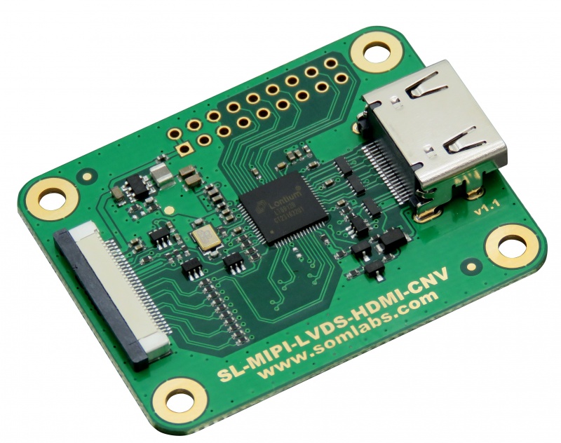
SL-MIPI-LVDS-HDMI-CNV (MIPI-DSI to LVDS HDMI converter) is flexible MIPI-DSI to LVDS and/or HDMI converter. The solution we dedicate to SoMLabs carrier boards equipped with MIPI-DSI interface (with FPC30 connector). Converter is fully compliant with DSI1.02 and HDMI1.4 and converts video stream up to 1080p @60Hz/8b.
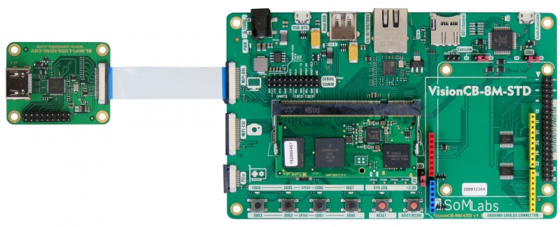
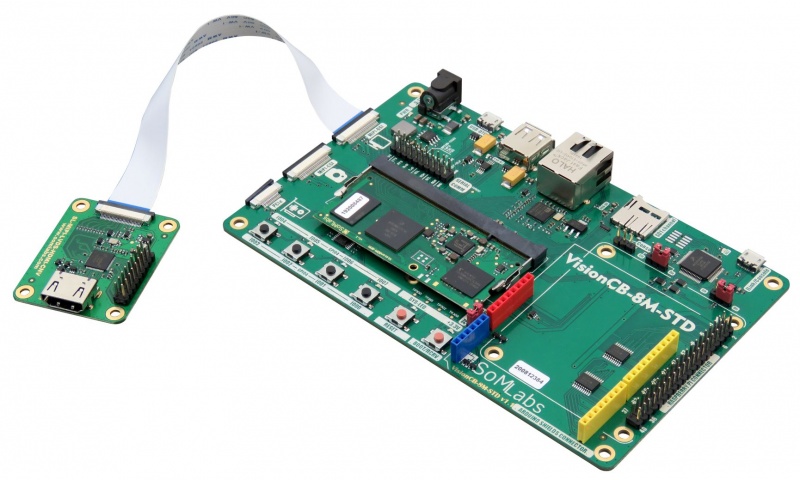
SL-MIPI-LVDS-HDMI-CNV is fully compatible with SoMLabs carrier borads equipeed with MIPI-DSI FPC30 connector.
Features
- MIPI-DSI to LVDS and/or HDMI display converter
- Integrated D-PHY1.1 (DSI1.02)
- From 1 up to 4 MIPI input data lanes
- Compatible with MIPI-DSI data packets: 18bpp, RGB666 and 24bpp RGB888
- Input bandwidth up tp 6Gb/s (4 lanes)
- LVDS output clocking up to 154 MHz
- Fully compatible with SoMLabs carrier board:
- VisionCB-8M-STD (dedicated to i.MX8M mini multicore MPU)
- VisionCB-STM32MP1-STD (dedicated to STM32MP1 multicore MPU)
- Plug & Play solution for SoMLabs customers
- Integrated stereo audio channel
- Connection with carrier board using FPC30 cable A-A type
Pictures
Ordering info
SL-MIPI-LVDS-HDMI-CNV - FPC 30-pin flat cable (A-A) is included.
Operating ranges
| Parameter | Value | Unit | Comment |
|---|---|---|---|
| Power Supply | |
|
Powered from carrier board |
| Current | |
|
Maximum peak value |
| Environment temperature | oC | - |
Electrical parameters
| Signal name | Parameter | Value | Units | ||
|---|---|---|---|---|---|
| Min. | Typ. | Max. | |||
| +5V | Supply Voltage | 4.75 | 5.0 | 5.25 | V |
| +3.3V | Supply Voltage | 3.2 | 3.3 | 3.35 | V |
| I5V | Supply Current (5V) | 40 | 80 | 100 | mA |
| I3.3V | Supply Current (3.3V) | 1 | 2.2 | 8 | mA |
| VIOI2C | I2C Input Voltage | 0 | 3.3 | 3.6 | V |
| VIORES/SPDIF | RES/SPDIF Input Voltage | 0 | 3.3 | 3.6 | V |
| fI2C | I2C Controller Speed | - | - | 400 | kHz |
| RINT | Interrupt Output Pull-up Resistance | - | 4.7 | - | kΩ |
| RI2C | I2C IOs Pull-up Resistance | - | 4.7 | - | kΩ |
MIPI-DSI (input) Pinout
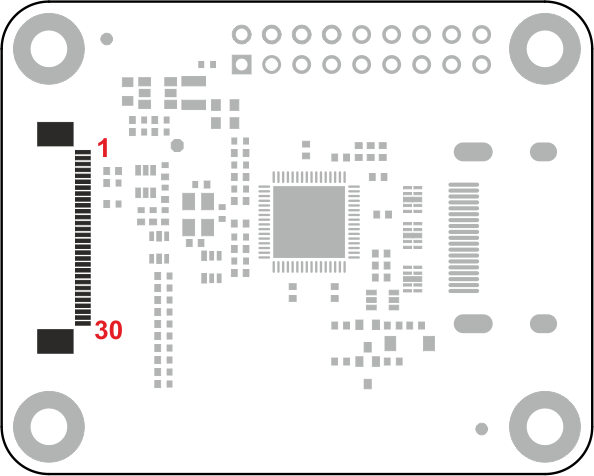
| FPC30 connector pin | Function name | Description |
|---|---|---|
| 1 | GND | - |
| 2 | - | - |
| 3 | HPD | HPD line from HDMI (voltage translated to 3.3V) |
| 4 | +5V | Power supply (input) |
| 5 | +5V | Power supply (input) |
| 6 | +3.3V | Power supply (input) |
| 7 | +3.3V | Power supply (input) |
| 8 | GND | - |
| 9 | SPDIF-TX | SPDIF input from SBC |
| 10 | INT | Interrupt output (voltage translated to 3.3V) |
| 11 | RESET | Reset input (voltage translated to 3.3V) |
| 12 | GND | - |
| 13 | SDA | I2C SDA line (voltage translated to 3.3V) |
| 14 | SCL | I2C SCL line (voltage translated to 3.3V) |
| 15 | GND | - |
| 16 | D3n | MIPI-DSI lane 3 negative line |
| 17 | D3p | MIPI-DSI lane 3 positive line |
| 18 | GND | - |
| 19 | D2n | MIPI-DSI lane 2 negative line |
| 20 | D2p | MIPI-DSI lane 2 positive line |
| 21 | GND | - |
| 22 | D1n | MIPI-DSI lane 1 negative line |
| 23 | D1p | MIPI-DSI lane 1 positive line |
| 24 | GND | - |
| 25 | D0n | MIPI-DSI lane 0 negative line |
| 26 | D0p | MIPI-DSI lane 0 positive line |
| 27 | GND | - |
| 28 | CLKn | MIPI-DSI clock negative line |
| 29 | CLKp | MIPI-DSI clock positive line |
| 30 | GND | - |
LVDS (output) Pinout
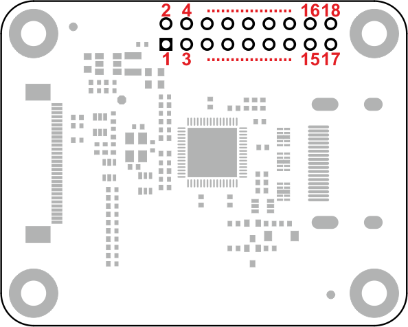
| LVDS connector pin | Function name | Description |
|---|---|---|
| 1 | +5V | Power supply for external devices (max. 20 mA) Internally connected with pin 2 |
| 2 | +5V | Power supply for external devices (max. 20 mA) Internally connected with pin 1 |
| 3 | - | - |
| 4 | GND | - |
| 5 | GND | - |
| 6 | GND | - |
| 7 | D0n | LVDS D0n data line |
| 8 | D0p | LVDS D0p data line |
| 9 | D1n | LVDS D1n data line |
| 10 | D1p | LVDS D1p data line |
| 11 | D2n | LVDS D2n data line |
| 12 | D2p | LVDS D2p data line |
| 13 | GND | - |
| 14 | GND | - |
| 15 | CLKn | LVDS CLKn clock line |
| 16 | CLKp | LVDS CLKp clock line |
| 17 | D3n | LVDS D3n data line |
| 18 | D3p | LVDS D3p data line |
HDMI (output) Pinout
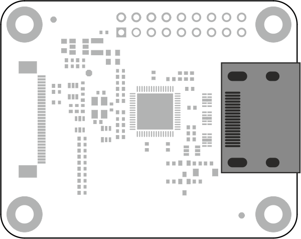
HDMI connector built-in SL-MIPI-LVDS-HDMI-CNV converter has standard HDMI pinout.
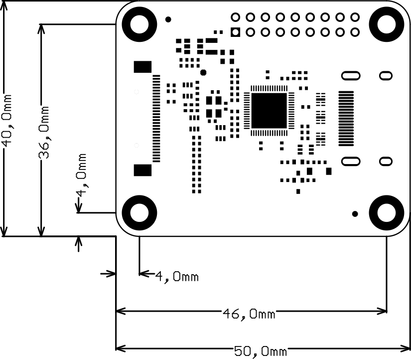
Dimensions

