VisionSOM-RT Datasheet and Pinout
From SomLabs Wiki

VisionSOM-RT Datasheet and Pinout
Contents
General description
The VisionSOM-RT family is a SODIMM-sized SoM based on the NXP i.MX RT application processor which features an advanced implementation of a single ARM Cortex-M7 core (at speeds up to 600MHz).
The VisionSOM-RT is a low power highly integrated SoM (System-on-Module) featuring high computation performance, real-time functionality and MCU usability. High security enabled by AES-128, HAB and On-the-fly QSPI Flash Decryption together with 2D graphical acceleration make an ideally suited solution for home and industrial control systems, wireless application, communication solutions and real-time systems.
The system supports industrial grade targeting embedded application.
SOMLabs also provides a complete hardware and software development board for the SoM in the form of a carrier board and optional TFT display and touch panel.
Applications
- Industrial embedded RTOS computer
- Home Appliances
- Home Automation – Smart Home
- Human-machine Interfaces (HMI)
- Point-of-sales (POS) terminals
- Cash Register
- 2D barcode scanners and printers
- Smart grid Infrastructure
- IoT gateways
- Residential getaways
- Machine vision equipment
- Robotics
- Fitness/outdoor equipment
Features
- Powered by NXP i.MX RT application processor
- Core clock up to 600MHz
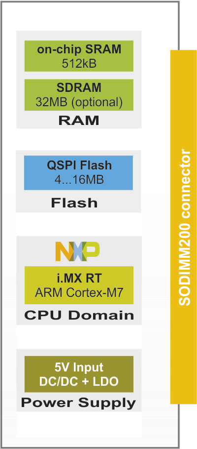
- 512kB on-chip RAM memory
- 256Mb (32MB) SDRAM memory
- 128Mb (16MB) QuadSPI Flash memory
- Power-efficient and cost-optimized solution
- Ideal for industrial IoT and embedded applications
- FreeRTOS support
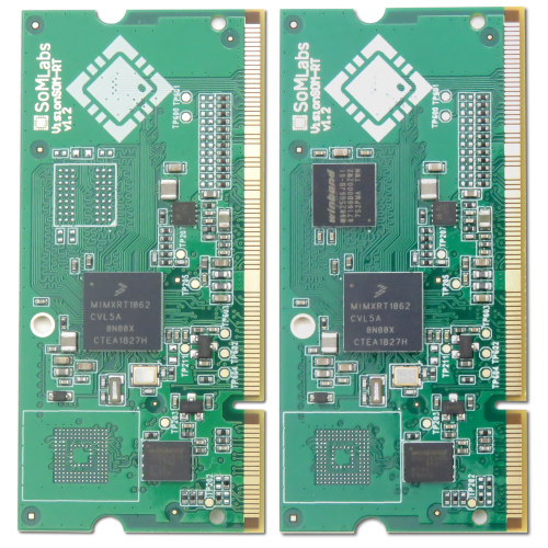
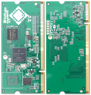
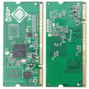
Pictures of SOM versions
| Version | Photo |
|---|---|
| RAM&QSPI | |
| QSPI |
Ordering info
| SLS | Product type SLS - System on Module |
| N | SOM Name 1 - VisionSOM SODIMM200 |
| 2 | CPU Family 2 - i.MX RT |
| CpuType | CPU Type RT52 - i.MX RT 1052 RT62 - i.MX RT 1062 |
| Clock | CPU Clock Speed 528C - 528MHz |
| RamSize | RAM Size 0R - No RAM 32R - 32MB |
| FlashSize | Flash Size Type and Density 4QSPI - 4MB QSPI Flash 16QSPI - 16MB QSPI Flash |
| SF | Special Features 0SF - No Special Features |
| TEMP | Operating Temperature C - Consumer: 0 to +70 C I - Industrial: -40 to +85 C |
| V | SOM Version A - Version 1.2 |
Block Diagram
Operating ranges
| Parameter | Value | Unit | Comment |
|---|---|---|---|
| Power Supply | |
|
Connected to +5VIN SODIMM pin |
| Input GPIO voltage | |
|
- |
| Environment temperature1 | |
oC | Industrial range |
| |
Consumer range |
Note:
1. Maximum MPU junction temperature is +105oC (industrial version) or +95oC (consumer version).
Electrical parameters
| SOM signal name |
Parameter | Value | Units | ||
|---|---|---|---|---|---|
| Min. | Typ. | Max. | |||
| +5VIN | Supply Voltage | 4.0 | 5.0 | 5.5 | V |
| - | Total Supply Current1 | x | x | x | A |
| VGPIO | GPIO Input Voltage | 0 | 3.3 | 3.62 | V |
| +3.3VOUT | SOM Internal LDO Output Current |
- | - | 0.5 | A |
| USB-OTGx-VBUS | USB Supply | 4.40 | - | 5.5 | V |
| VDD-COIN-3V | SNVS Backup Battery Supply |
2.66 | - | 3.6 | V |
| - | ADC Inputs Voltage | 0 | - | 3.3 | V |
Notes:
1. Excluding external load connected to +3.3VOUT lines.
2. Applying the maximum voltage 3.6V results in shorten lifetime. Recommended value is smaller than 3.5V.
Pinout
| "Function | | "i.MX-RT | | "Description | | Power | GND | - | - | | Power | GND | - | - | | Ctrl | PMIC-STBY-REQ | CCM_PMIC_STBY_REQ | Output, leave open if not used. | | Ctrl | POR-B | - | External warm reset input, active L. | | Ctrl | PMIC-ON-REQ | SNVS_PMIC_ON_REQ | Output, leave open if not used. | | Power | VDD-SNVS-3V3 | VDD_SNVS_IN | "SNVS backup power supply must be held between 2.9V and 3.3V if the system requires keeping real time and other data on OFF state. | | BOOT | BOOT-MODE1 | GPIO_AD_B0_05 | BOOT1 configuration line or multifunction GPIO with 3.3V logic levels. | | Power | VDD-COIN-3V | VDD_SNVS_IN | "Optional external coin battery for SNVS power domain, must be held between 2.9V and 3.3V if the system requires keeping real time and other data on OFF state. | | BOOT | BOOT-MODE0 | GPIO_AD_B0_04 | "BOOT1 configuration line or multifunction GPIO with 3.3V logic levels. | | NC | - | - | Not internally connected. | | USB | USB-OTG2-VBUS | USB_OTG2_VBUS | +5V USB bus. Leave open if not used. | | NC | - | - | Not internally connected. | | USB | USB-OTG1-VBUS | USB_OTG1_VBUS | +5V USB bus. Leave open if not used. | | Ctrl | ONOFF | ONOFF | Input for power interrupt generation. Leave open if not used. | | Power | GND | - | - | | Ctrl | POR-B | POR_B | "Cold reset negative logic input resets all modules and logic in the IC. | | Power | GND | - | - | | NC | - | - | Not internally connected. | | USB | USB-OTG2-DP | USB_OTG2_DP | Leave open if not used. | | Power | GND | - | - | | USB | USB-OTG2-DN | USB_OTG2_DN | Leave open if not used. | | Power | GND | - | - | | Power | GND | - | - | | NC | - | - | Not internally connected. | | USB | USB-OTG1-DP | USB_OTG1_DP | Leave open if not used. | | Power | GND | - | - | | USB | USB-OTG1-DN | USB_OTG1_DN | Leave open if not used. | | Power | GND | - | - | | Power | GND | - | - | | NC | - | - | Not internally connected. | | USB | nUSB-OTG-CHD | USB_OTG1_CHD_B | Leave open if not used. | | - | - | - | Not internally connected. | | JTAG | JTAG-MOD | GPIO_AD_B0_08 | "JTAG mode selector. | | - | - | - | Not internally connected. | | Power | GND | - | - | | - | - | - | Not internally connected. | | | CLK1-N | CCM_CLK1_N | "General purpose differential high speed clock input/output. | | Power | GND | - | - | | | CLK1-P | CCM_CLK1_P | "General purpose differential high speed clock input/output. | | Power | GND | - | - | | Power | GND | - | - | | NC | - | - | Not internally connected. | | JTAG | JTAG-TDI | GPIO_AD_B0_09 | "JTAG TDI input line. | | NC | - | - | Not internally connected. | | GPIO | GPIO-B1-09 | GPIO_AD_B1_09 | Multifunction GPIO with 3.3V logic levels. | | JTAG | JTAG-TMS | GPIO_AD_B0_06 | "JTAG TMS input line. | | GPIO | GPIO-4 | GPIO_AD_B0_04 | "Multifunction GPIO with 3.3V logic levels. | | JTAG | JTAG-nTRST | GPIO_AD_B0_11 | "JTAG nTRST input line. | | GPIO | GPIO-B1-11 | GPIO_AD_B1_11 | Multifunction GPIO with 3.3V logic levels. | | Power | GND | - | - | | Power | GND | - | - | | JTAG | JTAG-TDO | GPIO_AD_B0_10 | "JTAG TDO ouput line. | | GPIO | ENET-MDC | GPIO_EMC_40 | Multifunction GPIO with 3.3V logic levels. | | JTAG | JTAG-TCK | GPIO_AD_B0_07 | "JTAG TCK input line. | | GPIO | GPIO-3 | GPIO_AD_B0_03 | Multifunction GPIO with 3.3V logic levels. | | GPIO | GPIO-B1-14 | GPIO_AD_B1_14 | Multifunction GPIO with 3.3V logic levels. | | COM-GPIO | UART1-TXD | GPIO_AD_B0_12 | "UART1 TxD output | | GPIO | GPIO-2 | GPIO_AD_B0_02 | Multifunction GPIO with 3.3V logic levels. | | Power | GND | - | - | | Power | GND | - | - | | GPIO | ENET-MDIO | GPIO_EMC_41 | Multifunction GPIO with 3.3V logic levels. | | GPIO | GPIO-1 | GPIO_AD_B0_01 | Multifunction GPIO with 3.3V logic levels. | | COM-GPIO | UART1-RXD | GPIO_AD_B0_13 | "UART1 RxD input | | GPIO | GPIO-0 | GPIO_AD_B0_00 | Multifunction GPIO with 3.3V logic levels. | | COM-GPIO | UART2-TXD | GPIO_AD_B1_02 | "UART2 TxD output | | COM-GPIO | UART1-CTS | GPIO_AD_B0_14 | "UART1 CTS output | | COM-GPIO | UART2-RXD | GPIO_AD_B1_03 | "UART2 RxD input | | COM-GPIO | UART5-RXD | GPIO_B1_13 | "UART5 RxD input | | COM-GPIO | UART3-TXD | GPIO_AD_B1_06 | "UART3 TxD input | | Power | GND | - | - | | Power | GND | - | - | | COM-GPIO | UART2-CTS | GPIO_AD_B1_00 | "UART2 CTS output | | COM-GPIO | UART3-RXD | GPIO_AD_B1_07 | "UART3 RxD input | | COM-GPIO | UART1-RTS | GPIO_AD_B0_15 | "UART1 RTS input | | NC | - | - | Not internally connected. | | COM-GPIO | UART3-CTS | GPIO_AD_B1_04 | "UART3 CTS output | | NC | - | - | Not internally connected. | | COM-GPIO | UART2-RTS | GPIO_AD_B1_01 | "UART2 RTS input | | COM-GPIO | UART5-TXD | GPIO_B1_12 | "UART5 TxD output | | COM-GPIO | UART3-RTS | GPIO_AD_B1_05 | "UART3 RTS input | | Power | GND | - | - | | Power | GND | - | - | | NC | - | - | Not internally connected. | | Power | GND | - | - | | Power | +3.3VOUT | - | +3.3V generated by SOM's LDO. | | NC | - | - | Not internally connected. | | Power | +3.3VOUT | - | +3.3V generated by SOM's LDO. | | Power | +3.3VOUT | - | +3.3V generated by SOM's LDO. | | Power | +3.3VOUT | - | +3.3V generated by SOM's LDO. | | Power | +3.3VOUT | - | +3.3V generated by SOM's LDO. | | Power | +3.3VOUT | - | +3.3V generated by SOM's LDO. | | Power | +3.3VOUT | - | +3.3V generated by SOM's LDO. | | Power | +3.3VOUT | - | +3.3V generated by SOM's LDO. | | NC | - | - | Not internally connected. | | NC | - | - | Not internally connected. | | Power | +5VIN | - | +4.0-5.5V input power supply. | | Ethernet | ENET1-RXD0 | GPIO_B1_04 | Ethernet MAC1-PHY interface signal or multifunction GPIO with 3.3V logic levels. | | Power | +5VIN | - | +4.0-5.5V input power supply. | | Ethernet | ENET1-RXD1 | GPIO_B1_05 | Ethernet MAC1-PHY interface signal or multifunction GPIO with 3.3V logic levels. | | Power | +5VIN | - | +4.0-5.5V input power supply. | | Ethernet | ENET1-CRS-DV | GPIO_B1_06 | Ethernet MAC1-PHY interface signal or multifunction GPIO with 3.3V logic levels. | | Power | +5VIN | | +4.0-5.5V input power supply. | | Power | GND | - | - | | Power | +5VIN | | +4.0-5.5V input power supply. | | NC | - | - | Not internally connected. | | Power | +5VIN | | +4.0-5.5V input power supply. | | Power | GND | - | - | | Power | +5VIN | | +4.0-5.5V input power supply. | | NC | - | - | Not internally connected. | | Power | +5VIN | - | +4.0-5.5V input power supply. | | Ethernet | ENET2-RXD0 | GPIO_AD_B1_14 | Ethernet MAC2-PHY interface signal or multifunction GPIO with 3.3V logic levels. | | Power | +5VIN | - | +4.0-5.5V input power supply. | | NC | - | - | Not internally connected. | | Ethernet | ENET1-TXEN | GPIO_B1_09 | Ethernet MAC1-PHY interface signal or multifunction GPIO with 3.3V logic levels. | | Power | GND | - | - | | Power | GND | - | - | | Ethernet | ENET2-CRS-DV | GPIO_AD_B1_15 | Ethernet MAC2-PHY interface signal or multifunction GPIO with 3.3V logic levels. | | Ethernet | ENET1-TX-CLK | GPIO_B1_10 | "Ethernet MAC1-PHY interface signal or multifunction GPIO with 3.3V logic levels. | | Ethernet | ENET2-TXD1 | GPIO_AD_B1_13 | Ethernet MAC2-PHY interface signal or multifunction GPIO with 3.3V logic levels. | | Power | GND | - | - | | Ethernet | ENET2-TXEN | GPIO_AD_B1_12 | Ethernet MAC2-PHY interface signal or multifunction GPIO with 3.3V logic levels. | | Ethernet | ENET1-TXD0 | GPIO_B1_07 | Ethernet MAC1-PHY interface signal or multifunction GPIO with 3.3V logic levels. | | Ethernet | ENET2-TXD0 | GPIO_B1_15 | Ethernet MAC2-PHY interface signal or multifunction GPIO with 3.3V logic levels. | | Ethernet | ENET1-TXD1 | GPIO_B1_08 | Ethernet MAC1-PHY interface signal or multifunction GPIO with 3.3V logic levels. | | Power | GND | - | - | | Ethernet | ENET1-RXER | GPIO_B1_11 | Ethernet MAC1-PHY interface signal or multifunction GPIO with 3.3V logic levels. | | Power | GND | - | - | | Power | GND | - | - | | LCD | LCD-DATA21 | GPIO_B1_01 | LCD interface signal or multifunction GPIO with 3.3V logic levels. | | Power | GND | - | - | | LCD | LCD-DATA22 | GPIO_B1_02 | LCD interface signal or multifunction GPIO with 3.3V logic levels. | | Power | GND | - | - | | LCD | LCD-DATA17 | GND | Internally connected to GND. | | LCD | LCD-DATA23 | GPIO_B1_03 | LCD interface signal or multifunction GPIO with 3.3V logic levels. | | Power | GND | - | - | | Power | GND | - | - | | LCD | LCD_DATA18 | GND | Internally connected to GND. | | LCD | LCD-DATA19 | GPIO_B0_15 | LCD interface signal or multifunction GPIO with 3.3V logic levels. | | LCD | LCD-DATA13 | GPIO_B0_12 | LCD interface signal or multifunction GPIO with 3.3V logic levels. | | LCD | LCD-DATA20 | GPIO_B1_00 | LCD interface signal or multifunction GPIO with 3.3V logic levels. | | LCD | LCD-DATA14 | GPIO_B0_13 | LCD interface signal or multifunction GPIO with 3.3V logic levels. | | LCD | LCD-DATA15 | GPIO_B0_14 | LCD interface signal or multifunction GPIO with 3.3V logic levels. | | LCD | LCD_DATA8 | GND | Internally connected to GND. | | LCD | LCD-DATA16 | GND | Internally connected to GND. | | LCD | LCD-DATA9 | GND | Internally connected to GND. | | Power | GND | - | - | | Power | GND | - | - | | LCD | LCD-DATA11 | GPIO_B0_10 | LCD interface signal or multifunction GPIO with 3.3V logic levels. | | LCD | LCD-DATA5 | GPIO_B0_06 | LCD interface signal or multifunction GPIO with 3.3V logic levels. | | LCD | LCD-DATA12 | GPIO_B0_11 | LCD interface signal or multifunction GPIO with 3.3V logic levels. | | LCD | LCD-DATA6 | GPIO_B0_07 | LCD interface signal or multifunction GPIO with 3.3V logic levels. | | LCD | LCD-DATA10 | GPIO_B0_09 | LCD interface signal or multifunction GPIO with 3.3V logic levels. | | LCD | LCD-DATA0 | GND | Internally connected to GND. | | LCD | LCD-DATA3 | GPIO_B0_04 | LCD interface signal or multifunction GPIO with 3.3V logic levels. | | LCD | LCD-DATA1 | GND | Internally connected to GND. | | Power | GND | - | - | | LCD | LCD-RESET | GPIO_AD_B1_08 | LCD interface signal or multifunction GPIO with 3.3V logic levels. | | LCD | LCD-DATA4 | GPIO_B0_05 | LCD interface signal or multifunction GPIO with 3.3V logic levels. | | Power | GND | - | - | | LCD | LCD-HSYNC | GPIO_B0_02 | LCD interface signal or multifunction GPIO with 3.3V logic levels. | | LCD | LCD-CLK | GPIO_B0_00 | LCD interface signal or multifunction GPIO with 3.3V logic levels. | | LCD | LCD-VSYNC | GPIO_B0_03 | LCD interface signal or multifunction GPIO with 3.3V logic levels. | | LCD | LCD-ENABLE | GPIO_B0_01 | LCD interface signal or multifunction GPIO with 3.3V logic levels. | | LCD | LCD-DATA2 | GND | Internally connected to GND. | | Power | GND | - | - | | LCD | LCD-DATA7 | GPIO_B0_08 | LCD interface signal or multifunction GPIO with 3.3V logic levels. | | SDIO | SDIO1-D0 | GPIO_SD_B0_02 | SDIO interface signal or multifunction GPIO with 3.3V logic levels. | | NC | - | - | Not internally connected. | | SDIO | SDIO1-D3 | GPIO_SD_B0_05 | SDIO interface signal or multifunction GPIO with 3.3V logic levels. | | NC | - | - | Not internally connected. | | SDIO | SDIO1-D1 | GPIO_SD_B0_03 | SDIO interface signal or multifunction GPIO with 3.3V logic levels. | | NC | - | - | Not internally connected. | | SDIO | SDIO1-CMD | GPIO_SD_B0_00 | SDIO interface signal or multifunction GPIO with 3.3V logic levels. | | NC | - | - | Not internally connected. | | SDIO | SDIO1-D2 | GPIO_SD_B0_04 | SDIO interface signal or multifunction GPIO with 3.3V logic levels. | | NC | - | - | Not internally connected. | | Power | GND | - | - | | NC | - | - | Not internally connected. | | SDIO | SDIO1-CLK | GPIO_SD_B0_01 | SDIO interface signal or multifunction GPIO with 3.3V logic levels. | | NC | - | - | Not internally connected. | | Power | GND | - | - | | NC | - | - | Not internally connected. | | NC | - | - | Not internally connected. | | Power | GND | - | - | | Power | GND | - | - | | NC | | - | Not internally connected. | | NC | | - | Not internally connected. | | NC | - | - | Not internally connected. | | Power | GND | - | - | | NC | - | - | Not internally connected. | | NC | - | - | Not internally connected. | | NC | - | - | Not internally connected. | | NC | - | - | Not internally connected. | | NC | - | - | Not internally connected. | | NC | - | - | Not internally connected. | | NC | - | - | Not internally connected. | | NC | - | - | Not internally connected. | | NC | - | - | Not internally connected. | | Power | GND | - | - | | Power | GND | - | - |
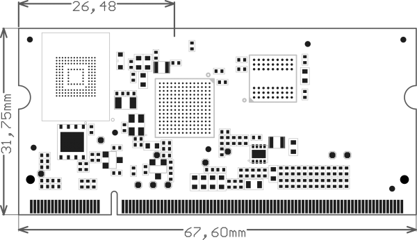
} Dimensions |

