SL-MIPI-CSI-OV5640 Datasheet and Pinout: Difference between revisions
From SomLabs Wiki
| (21 intermediate revisions by the same user not shown) | |||
| Line 28: | Line 28: | ||
* Built-in SL1 PMIC (developed by SoMLabs) | * Built-in SL1 PMIC (developed by SoMLabs) | ||
* Connection with carrier board using FPC30 cable | * Connection with carrier board using FPC30 cable | ||
<br>Note: fish-eye camera lens distorts the picture perspective. Example below. | |||
<br>[[File:fish-eye-view.jpg|900px|center]] | |||
== Pictures == | == Pictures == | ||
| Line 46: | Line 50: | ||
|- | |- | ||
| Power Supply | | Power Supply | ||
| <center>3.3 | | <center>3.3</center> | ||
| <center>V</center> | | <center>V</center> | ||
| Powered from carrier board | | Powered from carrier board | ||
|- | |- | ||
| Current | | Current | ||
| <center>0. | | <center>0.16</center> | ||
| <center>A</center> | | <center>A</center> | ||
| Maximum peak value | | Maximum peak value | ||
|- | |- | ||
| | |Working temperature | ||
|<center>- | |<center>-30…+70</center> | ||
|<sup>o</sup>C | |<sup>o</sup>C | ||
| - | | - | ||
| Line 71: | Line 75: | ||
| Typ. | | Typ. | ||
| Max. | | Max. | ||
|- | |- | ||
| +3.3V | | +3.3V | ||
| Line 85: | Line 82: | ||
| 3.35 | | 3.35 | ||
| V | | V | ||
|- | |- | ||
| I<sub>3.3V</sub> | | I<sub>3.3V</sub> | ||
| Supply Current (3.3V) | | Supply Current (3.3V) | ||
| | | 0.11 | ||
| | | .16 | ||
| | | - | ||
| mA | | mA | ||
|- | |- | ||
| | | t<sub>PWRSEQ</sub> | ||
| | | PMIC power-up time | ||
| | | - | ||
| | | 150 | ||
| | | - | ||
| | | ms | ||
|- | |- | ||
| VIO | | VIO | ||
| RES | | I2C, RES, PWDN Input Voltage | ||
| 0 | | 0 | ||
| 3.3 | | 3.3 | ||
| 3. | | 3.5 | ||
| V | | V | ||
|- | |- | ||
| Line 121: | Line 112: | ||
| kHz | | kHz | ||
|- | |- | ||
| R<sub> | | R<sub>I2C</sub> | ||
| | | I2C IOs Pull-up Resistance | ||
| - | | - | ||
| | | 10 | ||
| - | | - | ||
| kΩ | | kΩ | ||
|- | |- | ||
| R<sub> | | R<sub>PWDN</sub> | ||
| | | Serial resistors voltage divider connected between FPC30 pin and PWDN input of OV5640 sensor | ||
| - | | - | ||
| | | 2x10 | ||
| - | | - | ||
| kΩ | | kΩ | ||
|} | |} | ||
== MIPI- | == MIPI-CSI (output) Pinout == | ||
<br> | <br> | ||
[[File: | [[File:SL-MIPI-CSI-OV5640-conn.png|center]] | ||
<br /> | <br /> | ||
<br> | <br> | ||
| Line 155: | Line 146: | ||
|- | |- | ||
| 3 | | 3 | ||
| | | - | ||
| | | - | ||
|- | |- | ||
| 4 | | 4 | ||
| | | - | ||
| | | - | ||
|- | |- | ||
| 5 | | 5 | ||
| | | - | ||
| | | - | ||
|- | |- | ||
| 6 | | 6 | ||
| +3.3V | | +3.3V | ||
| Power supply | | Power supply | ||
|- | |- | ||
| 7 | | 7 | ||
| +3.3V | | +3.3V | ||
| Power supply | | Power supply | ||
|- | |- | ||
| 8 | | 8 | ||
| Line 179: | Line 170: | ||
|- | |- | ||
| 9 | | 9 | ||
| | | - | ||
| | | - | ||
|- | |- | ||
| 10 | | 10 | ||
| | | PWDN | ||
| | | OV5640 - Power Down input (active high, internal pull-down) | ||
|- | |- | ||
| 11 | | 11 | ||
| RESET | | RESET | ||
| Reset input ( | | OV5640 - Reset input (active low, internal pull-up) | ||
|- | |- | ||
| 12 | | 12 | ||
| Line 195: | Line 186: | ||
|- | |- | ||
| 13 | | 13 | ||
| | | SIOD_C | ||
| I2C | | SCL line of configuration I2C interface (internal pull-up) | ||
|- | |- | ||
| 14 | | 14 | ||
| | | SIO_D | ||
| I2C | | SDA line of configuration I2C interface (internal pull-up) | ||
|- | |- | ||
| 15 | | 15 | ||
| Line 207: | Line 198: | ||
|- | |- | ||
| 16 | | 16 | ||
| | | - | ||
| | | - | ||
|- | |- | ||
| 17 | | 17 | ||
| | | - | ||
| | | - | ||
|- | |- | ||
| 18 | | 18 | ||
| Line 219: | Line 210: | ||
|- | |- | ||
| 19 | | 19 | ||
| | | - | ||
| | | - | ||
|- | |- | ||
| 20 | | 20 | ||
| | | - | ||
| | | - | ||
|- | |- | ||
| 21 | | 21 | ||
| Line 231: | Line 222: | ||
|- | |- | ||
| 22 | | 22 | ||
| | | MDN1 | ||
| | | CSI_DATA1_n | ||
|- | |- | ||
| 23 | | 23 | ||
| | | MDP1 | ||
| | | CSI_DATA1_p | ||
|- | |- | ||
| 24 | | 24 | ||
| Line 243: | Line 234: | ||
|- | |- | ||
| 25 | | 25 | ||
| | | MDN0 | ||
| | | CSI_DATA0_n | ||
|- | |- | ||
| 26 | | 26 | ||
| | | MDP0 | ||
| | | CSI_DATA0_p | ||
|- | |- | ||
| 27 | | 27 | ||
| Line 255: | Line 246: | ||
|- | |- | ||
| 28 | | 28 | ||
| | | MCN | ||
| | | CSI_CLK_n | ||
|- | |- | ||
| 29 | | 29 | ||
| | | MCP | ||
| | | CSI_CLK_p | ||
|- | |- | ||
| 30 | | 30 | ||
| GND | | GND | ||
| - | | - | ||
|- | |- | ||
|} | |} | ||
== Dimensions == | == Dimensions == | ||
<br> | <br> | ||
[[File: | [[File:SL-MIPI-CSI-OV5640-dimension.png|center]] | ||
Latest revision as of 13:41, 27 November 2023

SL-MIPI-CSI-OV5640 5Mpx camera module with MIPI-CSI interface and OV5640 video sensor Datasheet and Pinout
General description
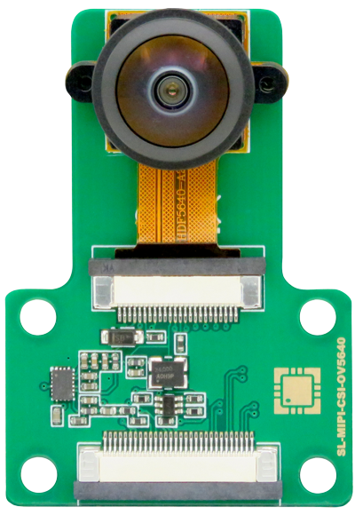
SL-MIPI-CSI-OV5640 is the 5 Mpx color camera module. Module is equipped with MIPI-CSI interface and FPC30 connector therefore SL-MIPI-CSI-OV5640 module is matched to the SoMLabs carrier boards.
The SL-MIPI-CSI-OV5640 is equipped with OV5640 hi-res HD 5 Mpx CMOS video sensor. Video interface is dual lane MIPI-CSI interface and module supports electronic shutter mode: rolling shutter/frame exposure.
As a result of using advanced PMIC – SL1 – developed by SoMLabs, the SL-MIPI-CSI-OV5640 module is powered from single +3.3V line available in FPC connector.
The SL-MIPI-CSI-OV5640 is fully compatible with SoMLabs carrier boards equipped with MIPI-CSI connectors. By default SL-MIPI-CSI-OV5640 module is equipped with fish-eye (120º) lens.
Features
- Based on OV5640 CMOS video chip
- Resolution 2592 x 1944 px
- Fish-eye lens (120º)
- Output formats: 8/10-b RGB RAW
- MIPI-CSI interface (2 lanes)
- Typical frame rates:
- QSXGA (2592×1944): 15 fps
- 1080p: 30 fps
- 1280×960: 45 fps
- 720p: 60 fps
- VGA (640×480): 90 fps
- QVGA (320×240): 120 fps
- Shutter: rolling/frame exposure
- Single rail +3.3V power supply
- Configuration via I2C
- Operating temperature -30÷+70°C
- Fully compatible with SoMLabs carrier boards equippped with MIPI-CSI interface (FPC30 connector)
- Built-in clock source
- Built-in SL1 PMIC (developed by SoMLabs)
- Connection with carrier board using FPC30 cable
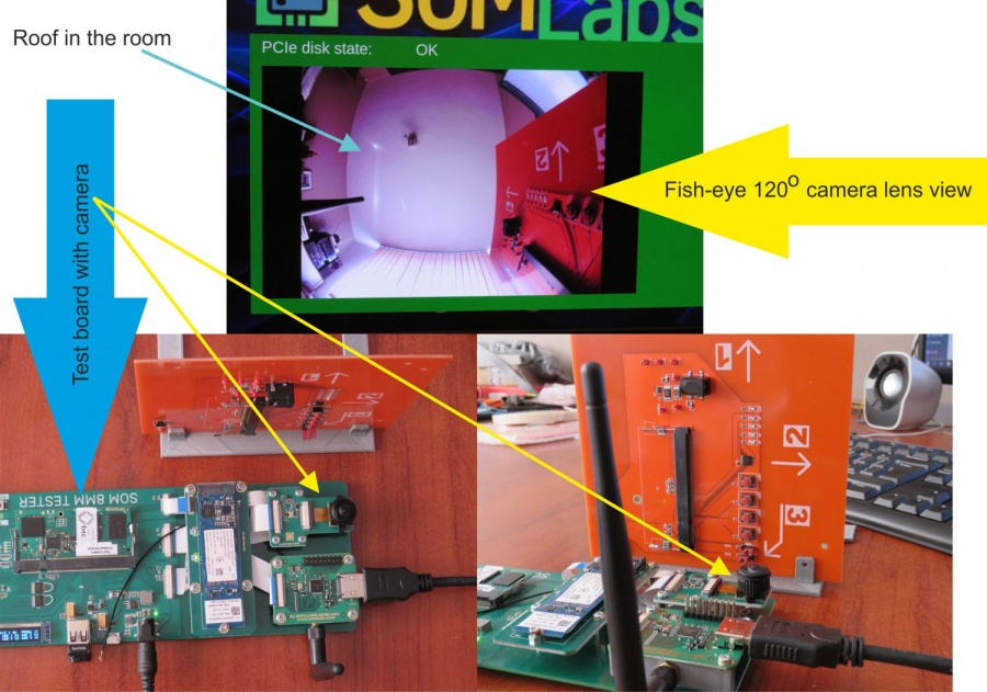
Note: fish-eye camera lens distorts the picture perspective. Example below.
Pictures
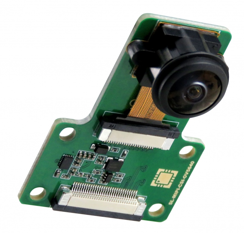
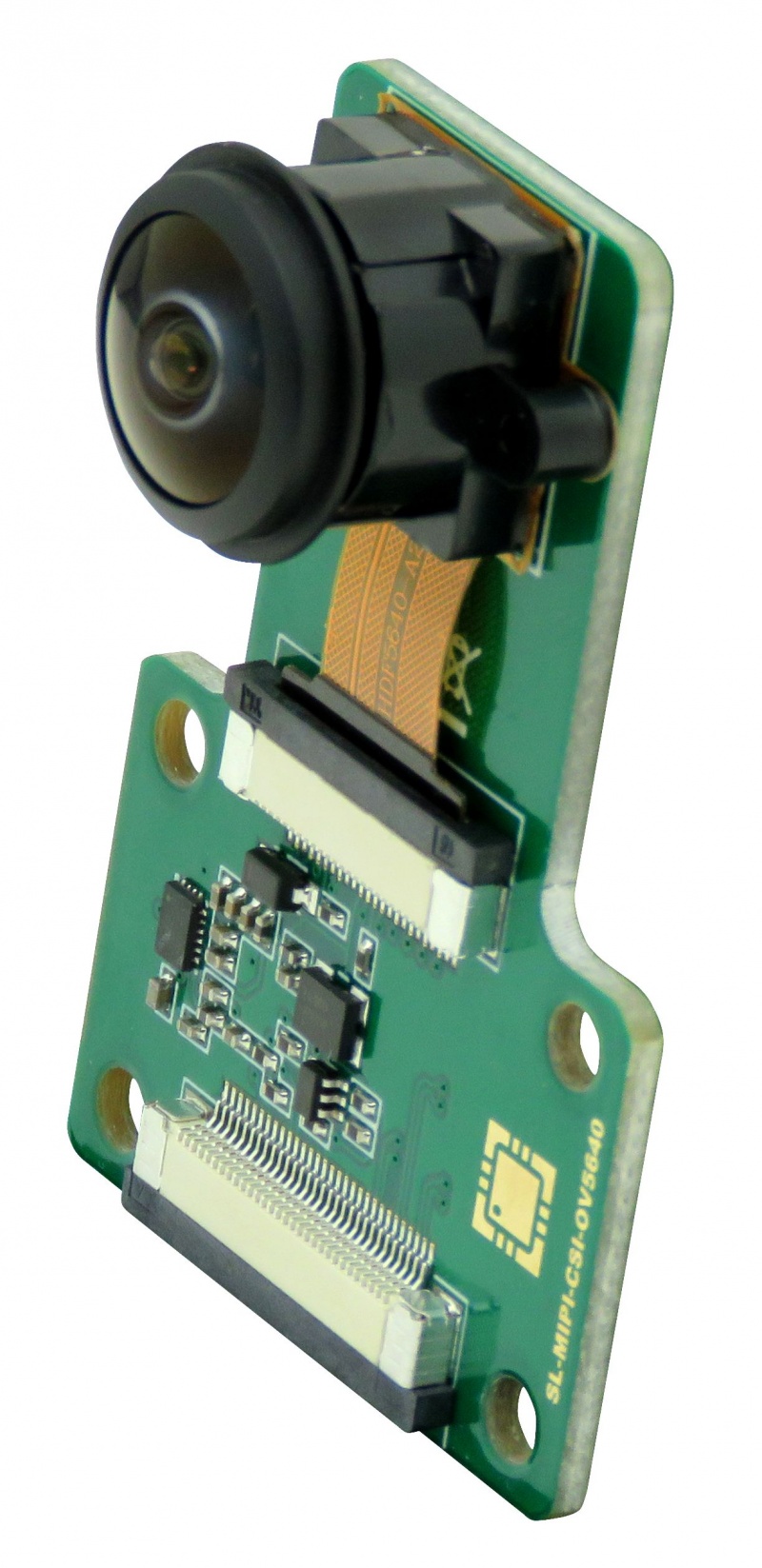
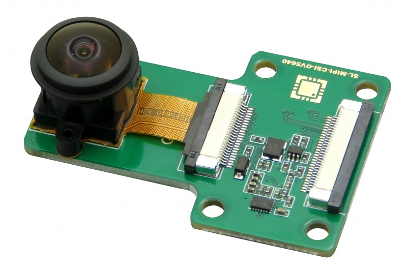
Ordering info
SL-MIPI-CSI-OV5640 - FPC 30-pin flat cable (A-A) is included.
Operating ranges
| Parameter | Value | Unit | Comment |
|---|---|---|---|
| Power Supply | Powered from carrier board | ||
| Current | Maximum peak value | ||
| Working temperature | oC | - |
Electrical parameters
| Signal name | Parameter | Value | Units | ||
|---|---|---|---|---|---|
| Min. | Typ. | Max. | |||
| +3.3V | Supply Voltage | 3.2 | 3.3 | 3.35 | V |
| I3.3V | Supply Current (3.3V) | 0.11 | .16 | - | mA |
| tPWRSEQ | PMIC power-up time | - | 150 | - | ms |
| VIO | I2C, RES, PWDN Input Voltage | 0 | 3.3 | 3.5 | V |
| fI2C | I2C Controller Speed | - | - | 400 | kHz |
| RI2C | I2C IOs Pull-up Resistance | - | 10 | - | kΩ |
| RPWDN | Serial resistors voltage divider connected between FPC30 pin and PWDN input of OV5640 sensor | - | 2x10 | - | kΩ |
MIPI-CSI (output) Pinout
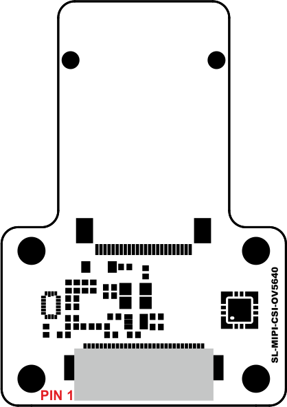
| FPC30 connector pin | Function name | Description |
|---|---|---|
| 1 | GND | - |
| 2 | - | - |
| 3 | - | - |
| 4 | - | - |
| 5 | - | - |
| 6 | +3.3V | Power supply |
| 7 | +3.3V | Power supply |
| 8 | GND | - |
| 9 | - | - |
| 10 | PWDN | OV5640 - Power Down input (active high, internal pull-down) |
| 11 | RESET | OV5640 - Reset input (active low, internal pull-up) |
| 12 | GND | - |
| 13 | SIOD_C | SCL line of configuration I2C interface (internal pull-up) |
| 14 | SIO_D | SDA line of configuration I2C interface (internal pull-up) |
| 15 | GND | - |
| 16 | - | - |
| 17 | - | - |
| 18 | GND | - |
| 19 | - | - |
| 20 | - | - |
| 21 | GND | - |
| 22 | MDN1 | CSI_DATA1_n |
| 23 | MDP1 | CSI_DATA1_p |
| 24 | GND | - |
| 25 | MDN0 | CSI_DATA0_n |
| 26 | MDP0 | CSI_DATA0_p |
| 27 | GND | - |
| 28 | MCN | CSI_CLK_n |
| 29 | MCP | CSI_CLK_p |
| 30 | GND | - |
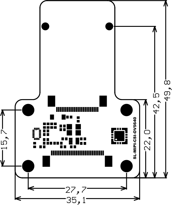
Dimensions
