StarSBC-6ULL Datasheet and Pinout
From SomLabs Wiki

StarSBC-6ULL Datasheet and Pinout
General description
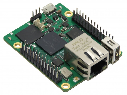
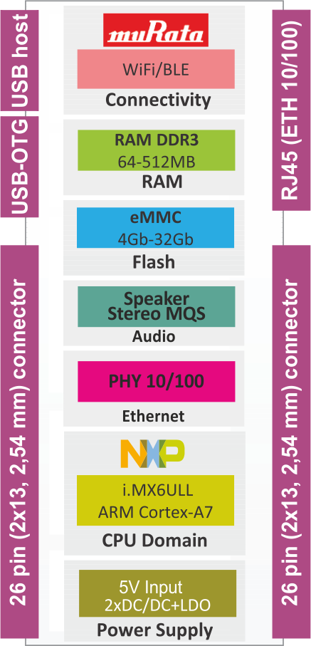
The StarSBC-6ULL SBC (Single Board Computer) is small but powerful IoT Sensor Hub, optimized for operation in applications requiring a large number of communication interfaces. The StarSBC-6ULL is equipped with on-board PHY 10/100 Mb/s Ethernet interface, Murata 1DX radio module (integrated WiFi/BLE), USB host and USB-OTG interfaces. The StarSBC-6ULL supports connections to a variety of interfaces: I2C, SPI, UART and CAN. Additionally the StarSBC-6ULL module is equipped with easy to use 2×26 pin connectors with 40 GPIOs for any use in user application.
The StarSBC-6ULL can be optionally equipped with communication expander module SLH2-comm, which is equipped with 2 x CAN, 2 x RS485, 2 x RS232 physical layers interfaces.
The StarSBC-6ULL supports industrial grade embedded applications.
Applications
- IoT Sensor Hubs
- Home Appliances
- IoT gateways
- Home Automation – Smart Home
- Point-of-sales (POS) terminals
- Cash Register
- 2D barcode scanners and printers
- Smart grid infrastructure
- Residential gateways
- Outdoor equipment
Features
- Powered by NXP i.MX 6ULL application processor
- Core clock up to 900MHz
- Up to 1GB RAM DDR3L
- Up to 32GB eMMC
- Optional Murata 802.11b/g/n Wi-Fi and Bluetooth v5.1 module
- Power-efficient and cost-optimized solution
- Ideal for industrial IoT and embedded applications
- Integrated security features
Pictures of SBC versions
| Version | Photo |
|---|---|
| eMMC |
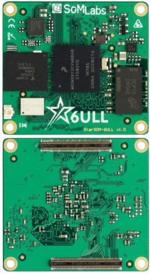 |
| Wi-Fi and Ethernet PHY10/100 are available as an options. |
Ordering info
| SLS | Product type SLS - System on Module |
| 0 | SOM Name 0 - StarSOM board-to-board connectors |
| 6 | CPU Family 6 - i.MX6 |
| Y2 | CPU Type Y2 - i.MX6 ULL Y2 |
| Clock | CPU Clock Speed 528C - 528MHz 792C - 792MHz 900C - 900MHz |
| RamSize | DDR3 RAM Size 128R - 128MB 256R - 256MB 512R - 512MB |
| FlashSize | Flash Size Type and Density 04GE - 4GB eMMC 08GE - 8GB eMMC 16GE - 16GB eMMC 32GE - 32GB eMMC |
| SF | Special Features 0SF - No Special Features 1WB - Built-in Murata 802.11b/g/n Wi-Fi and Bluetooth v5.1 Module 2ET - Built-in Microchip 100Mb Ethernet PHY 3WE - Built-in Murata 802.11b/g/n Wi-Fi/Bluetooth v5.1 and Microchip 100Mb Ethernet PHY |
| TEMP | Operating Temperature C - Consumer: 0 to +70 C E - Extended with Wi-Fi: -25 to +70 C I - Industrial: -40 to +85 C |
Block Diagram
Operating ranges
| Parameter | Value | Unit | Comment |
|---|---|---|---|
| Power Supply | Connected to +3V3IN pins | ||
| Input GPIO voltage | - | ||
| Environment temperature1 | oC | Industrial range w/o WiFi module | |
| Industrial range with WiFi module | |||
| Consumer range |
Note:
1. Maximum MPU junction temperature is +105oC (industrial version) or +95oC (consumer version).
Electrical parameters
| SOM signal name |
Parameter | Value | Units | ||
|---|---|---|---|---|---|
| Min. | Typ. | Max. | |||
| +3V3IN | Supply Voltage | 3.15 | 3.3 | 3.45 | V |
| +3V3IN | Total Supply Current1 | - | 175 | 255 | mA |
| VGPIO | GPIO Input Voltage | 0 | 3.3 | 3.62 | V |
| +3V3SW | Output current of 3.3V power supply for peripherals |
- | - | 0.2 | A |
| USB-OTGx-VBUS | USB Supply | 4.40 | - | 5.5 | V |
| VDD-COIN-3V | SNVS Backup Battery Supply |
2.66 | - | 3.6 | V |
| - | ADC Inputs Voltage | 0 | - | 3.3 | V |
Notes:
1. Excluding external load connected to +3.3VOUT lines.
2. Applying the maximum voltage 3.6V results in shorten lifetime. Recommended value is smaller than 3.5V.
SBC pinout
StarSOM-6ULL board-to-board connectors view (top view)
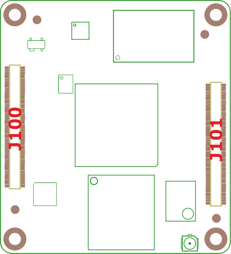
| SoM pin number | Default function | GPIO | BGA289 ball | Notes |
|---|---|---|---|---|
| 1 | GND | - | - | |
| 2 | GND | - | - | |
| 26 | LCD.RES | GPIO3.04 | E9 | |
| 28 | I2C2.SDA | GPIO1.31 | G13 | Internally pull-uped with 4.7k connected to 3.3V |
| 30 | I2C2.SCL | GPIO1.30 | F17 | Internally pull-uped with 4.7k connected to 3.3V |
| 32 | GPIO1.01 | GPIO1.01 | L15 | |
| 34 | GPIO1.02 | GPIO1.02 | L14 | |
| 36 | GPIO1.03 | GPIO1.03 | L17 | |
| 38 | GPIO1.04 | GPIO1.04 | M16 | |
| 39 | GND | - | - | |
| 40 | GND | - | - | |
| 41 | VDD.EMMC | - | - | Internal 1.8V LDO output as reference or power supply voltage for QSPI (SDIO) interface |
| 42 | LCD.CLK | GPIO3.00 | A8 | |
| 43 | QSPI.CLK | GPIO4.11 | D5 | Line referenced to VDD.EMMC power supply (1.8V) |
| 44 | GND | - | - | |
| 45 | QSPI.CS0 | GPIO4.16 | E6 | Line referenced to VDD.EMMC power supply (1.8V) |
| 46 | LCD.VSYNC | GPIO3.03 | C9 | |
| 47 | QSPI.D0 | GPIO4.12 | A3 | Line referenced to VDD.EMMC power supply (1.8V) |
| 48 | LCD.HSYNC | GPIO3.02 | D9 | |
| 49 | QSPI.D1 | GPIO4.13 | C5 | Line referenced to VDD.EMMC power supply (1.8V) |
| 50 | LCD.ENABLE | GPIO3.01 | B8 | |
| 51 | QSPI.D2 | GPIO4.14 | B5 | Line referenced to VDD.EMMC power supply (1.8V) |
| 52 | LCD.DATA23 | GPIO3.28 | B16 | |
| 53 | QSPI.D3 | GPIO4.15 | A4 | Line referenced to VDD.EMMC power supply (1.8V) |
| 54 | LCD.DATA22 | GPIO3.27 | A14 | |
| 55 | QSPI.DQS | GPIO4.10 | B4 | Line referenced to VDD.EMMC power supply (1.8V) |
| 56 | LCD.DATA21 | GPIO3.26 | B14 | |
| 57 | GND | - | - | |
| 58 | LCD.DATA20 | GPIO3.25 | C14 | |
| 59 | BT.PCMCLK | GPIO4.26 | D3 | BT-BLE interface connection (if 1DX modules used) If 1DX modules is not used alternative pin functions (incl. GPIO) available |
| 60 | LCD.DATA19 | GPIO3.24 | D14 | |
| 61 | BT.PCMOUT | GPIO4.27 | D2 | BT-BLE interface connection (if 1DX modules used) If 1DX modules is not used alternative pin functions (incl. GPIO) available |
| 62 | LCD.DATA18 | GPIO3.23 | A13 | |
| 63 | BT.PCMIN | GPIO4.28 | D1 | BT-BLE interface connection (if 1DX modules used) If 1DX modules is not used alternative pin functions (incl. GPIO) available |
| 64 | LCD.DATA17 | GPIO3.22 | B13 | |
| 65 | BT.PCMSYNC | GPIO4.25 | D4 | BT-BLE interface connection (if 1DX modules used) If 1DX modules is not used alternative pin functions (incl. GPIO) available |
| 66 | LCD.DATA16 | GPIO3.21 | C13 | |
| 67 | BT.RTS | GPIO4.23 | E2 | BT-BLE interface connection - UART5 (if 1DX modules used) If 1DX modules is not used alternative pin functions (incl. GPIO) available |
| 68 | LCD.DATA15 | GPIO3.20 | D13 | |
| 69 | BT.CTS | GPIO4.24 | E1 | BT-BLE interface connection - UART5 (if 1DX modules used) If 1DX modules is not used alternative pin functions (incl. GPIO) available |
| 70 | LCD.DATA14 | GPIO3.19 | A12 | |
| 71 | BT.TXD | GPIO4.22 | E3 | BT-BLE interface connection - UART5 (if 1DX modules used) If 1DX modules is not used alternative pin functions (incl. GPIO) available |
| 72 | LCD.DATA13 | GPIO3.18 | B12 | |
| 73 | BT.RXD | GPIO4.21 | E4 | BT-BLE interface connection - UART5 (if 1DX modules used) If 1DX modules is not used alternative pin functions (incl. GPIO) available |
| 74 | LCD.DATA12 | GPIO3.17 | C12 | |
| 75 | BT.WAKE | GPIO4.20 | F3 | BT-BLE interface connection (if 1DX modules used) If 1DX modules is not used alternative pin functions (incl. GPIO) available |
| 76 | LCD.DATA11 | GPIO3.16 | D12 | |
| 77 | BT.HWAKE | GPIO4.19 | F2 | BT-BLE interface connection (if 1DX modules used) If 1DX modules is not used alternative pin functions (incl. GPIO) available |
| 78 | LCD.DATA10 | GPIO3.15 | E12 | |
| 79 | BT.ENABLE | GPIO4.17 | F5 | BT-BLE interface connection (if 1DX modules used) If 1DX modules is not used alternative pin functions (incl. GPIO) available |
| 80 | LCD.DATA09 | GPIO3.14 | A11 | |
| 81 | WLAN.HWAKE | GPIO4.18 | E5 | WiFi interface connection (if 1DX modules used) If 1DX modules is not used alternative pin functions (incl. GPIO) available |
| 82 | LCD.DATA08 | GPIO3.13 | B11 | |
| 83 | WLAN.EN | GPIO1.08 | N17 | WiFi interface connection (if 1DX modules used) If 1DX modules is not used alternative pin functions (incl. GPIO) available |
| 84 | LCD.DATA07 | GPIO3.12 | D11 | |
| 85 | GND | - | - | |
| 86 | LCD.DATA06 | GPIO3.11 | A10 | |
| 87 | SDIO1.CLK | GPIO2.17 | C1 | WiFi interface connection (if 1DX modules used) If 1DX modules is not used alternative pin functions (incl. GPIO) available |
| 88 | LCD.DATA05 | GPIO3.10 | B10 | |
| 89 | SDIO1.CMD | GPIO2.16 | C2 | WiFi interface connection (if 1DX modules used) If 1DX modules is not used alternative pin functions (incl. GPIO) available |
| 90 | LCD.DATA04 | GPIO3.09 | C10 | |
| 91 | SDIO1.D2 | GPIO2.20 | B1 | WiFi interface connection (if 1DX modules used) If 1DX modules is not used alternative pin functions (incl. GPIO) available |
| 92 | LCD.DATA03 | GPIO3.08 | D10 | |
| 93 | SDIO1.D0 | GPIO2.18 | B3 | WiFi interface connection (if 1DX modules used) If 1DX modules is not used alternative pin functions (incl. GPIO) available |
| 94 | LCD.DATA02 | GPIO3.07 | E10 | |
| 95 | SDIO1.D3 | GPIO2.21 | A2 | WiFi interface connection (if 1DX modules used) If 1DX modules is not used alternative pin functions (incl. GPIO) available |
| 96 | LCD.DATA01 | GPIO3.06 | A9 | |
| 97 | SDIO1.D1 | GPIO2.19 | B2 | WiFi interface connection (if 1DX modules used) If 1DX modules is not used alternative pin functions (incl. GPIO) available |
| 98 | LCD.DATA00 | GPIO3.05 | B9 | |
| 99 | GND | - | - | |
| 100 | GND | - | - | |
| 1 | +3V3IN | - | - | External power supply 3.3V |
| 2 | +3V3IN | - | - | External power supply 3.3V |
| 3 | +3V3IN | - | - | External power supply 3.3V |
| 4 | +3V3IN | - | - | External power supply 3.3V |
| 5 | +3V3IN | - | - | External power supply 3.3V |
| 6 | +3V3IN | - | - | External power supply 3.3V |
| 7 | +3V3IN | - | - | External power supply 3.3V |
| 8 | +3V3IN | - | - | External power supply 3.3V |
| 9 | +3V3IN | - | - | External power supply 3.3V |
| 10 | +3V3IN | - | - | External power supply 3.3V |
| 11 | GND | - | - | |
| 12 | GND | - | - | |
| 13 | GND | - | - | |
| 14 | GND | - | - | |
| 15 | GND | - | - | |
| 16 | GND | - | - | |
| 17 | PMIC-ON-REQ | |||
| 18 | ON-OFF | ON-OFF | R8 | |
| 19 | PMIC-STBY-REQ | PMIC-STBY-REQ | U9 | |
| 20 | POR | POR | P8 | Power-on-reset input-output |
| 21 | VDD-3V3-SNVS | VDD-SNVS-IN | P12 | SNVS domain power supply External 3.3V connection power supply is necessary |
| 22 | RECOVERY | System recovery pin: RECOVERY=0 during reset -> start recovery mode RECOVERY=1 or not connected -> normal operation mode | ||
| 23 | GND | - | - | |
| 24 | RESET.IN | - | - | System reset |
| 25 | UART4.RXD | GPIO1.29 | G16 | Default Linux console RxD line |
| 26 | GND | - | - | |
| 27 | UART4.TXD | GPIO1.28 | G17 | Default Linux console TxD line |
| 28 | TAMPER.0 | GPIO5.00 | R10 | |
| 29 | +3V3SW | - | - | Reference 3.3V power supply for external peripherals, maximum load 200 mA |
| 30 | TAMPER.1 | GPIO5.01 | R9 | |
| 32 | TAMPER.2 | GPIO5.02 | P11 | |
| 34 | TAMPER.3 | GPIO5.03 | P10 | |
| 36 | TAMPER.4 | GPIO5.04 | P9 | |
| 37 | GND | - | - | |
| 38 | TAMPER.5 | GPIO5.05 | N8 | |
| 39 | USB2.VBUS | U12 | ||
| 40 | TAMPER.6 | GPIO5.06 | N11 | |
| 41 | USB2.DN | - | T13 | |
| 42 | TAMPER.7 | GPIO5.07 | N10 | |
| 43 | USB2.DP | - | U13 | |
| 44 | TAMPER.8 | GPIO5.08 | N9 | |
| 45 | GND | - | - | |
| 46 | TAMPER.9 | GPIO5.09 | R6 | |
| 47 | GPIO1.05 | GPIO1.05 | M17 | |
| 48 | GND | - | - | |
| 49 | USB1.VBUS | - | T12 | |
| 50 | JTAG.TCK | GPIO1.14 | M14 | Optionally used as 32kHz clock source for 1DX radio module |
| 51 | USB1.DN | - | T15 | |
| 52 | JTAG.TDI | GPIO1.13 | N16 | |
| 53 | USB1.DP | - | U15 | |
| 54 | JTAG.TDO | GPIO1.12 | N15 | |
| 55 | GND | - | - | |
| 56 | JTAG.TMS | GPIO1.11 | P14 | |
| 57 | USB1.ID | GPIO1.00 | K13 | |
| 58 | JTAG.TRST | GPIO1.15 | N14 | |
| 60 | GND | - | - | |
| 62 | UART1.CTS | GPIO1.18 | K15 | |
| 63 | GND | - | - | |
| 64 | UART1.RTS | GPIO1.19 | J14 | |
| 65 | ENET2.TX-CLK | GPIO2.14 | D17 | |
| 66 | UART1.RXD | GPIO1.17 | K16 | |
| 67 | ENET2.TXD1 | GPIO2.12 | A16 | |
| 68 | UART1.TXD | GPIO1.16 | K14 | |
| 69 | ENET2.TXD0 | GPIO2.11 | A15 | |
| 70 | UART2.CTS | GPIO1.22 | J15 | |
| 71 | ENET2.TXEN | GPIO2.13 | B15 | |
| 72 | UART2.RTS | GPIO1.23 | H14 | |
| 73 | ENET2.RXER | GPIO2.15 | D16 | |
| 74 | UART2.RXD | GPIO1.21 | J16 | |
| 75 | ENET2.RXEN | GPIO2.10 | B17 | |
| 76 | UART2.TXD | GPIO1.20 | J17 | |
| 77 | ENET2.RXD0 | GPIO2.08 | C17 | |
| 78 | UART3.CTS | GPIO1.26 | H15 | |
| 79 | ENET2.RXD1 | GPIO2.09 | C16 | |
| 80 | UART3.RTS | GPIO1.27 | G14 | |
| 81 | ENET.MDC | GPIO1.07 | L16 | |
| 82 | UART3.RXD | GPIO1.25 | H16 | |
| 83 | ENET.MDIO | GPIO1.06 | K17 | |
| 84 | UART3.TXD | GPIO1.24 | H17 | |
| 85 | GND | - | - | |
| 86 | GND | - | - | |
| 87 | ENET1.LED0 | - | - | LED0/nWAYEN - output PHY signal (LED cathode) |
| 89 | ENET1.LED1 | - | - | LED0/SPEED - output PHY signal (LED cathode) |
| 91 | ENET1.RXN | - | - | Rx_n - external Ethernet trafo connector |
| 93 | ENET1.RXP | - | - | Rx_p - external Ethernet trafo connector |
| 95 | ENET1.TXN | - | - | Tx_n - external Ethernet trafo connector |
| 97 | ENET1.TXP | - | - | Tx_p - external Ethernet trafo connector |
| 99 | GND | - | - | |
| 100 | GND | - | - | |
| - | JTAG.MOD | GPIO1.10 | P15 | Used as hardware reset Ethernet of PHY with 4.7k pull-down resistor |
| - | BOOT.MODE1 | - | U10 | Permanently connected to GND |
Dimensions
