SL-MIPI-LVDS-HDMI-CNV-11 Datasheet and Pinout
From SomLabs Wiki

SL-MIPI-LVDS-HDMI-CNV MIPI-DSI to LVDS and HDMI converter Datasheet and Pinout
General description
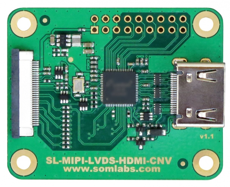
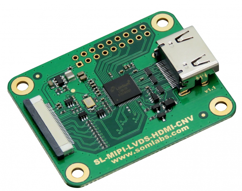
SL-MIPI-LVDS-HDMI-CNV (MIPI-DSI to LVDS HDMI converter) is flexible MIPI-DSI to LVDS and/or HDMI converter. The solution we dedicate to SoMLabs carrier boards equipped with MIPI-DSI interface (with FPC30 connector). Converter is fully compliant with DSI1.02 and HDMI1.4 and converts video stream up to 1080p @60Hz/8b.
SL-MIPI-LVDS-HDMI-CNV is fully compatible with SoMLabs carrier borads equipeed with MIPI-CSI FPC30 connector.
Features
- MIPI-DSI to LVDS and/or HDMI display converter
- Integrated D-PHY1.1 (DSI1.02)
- From 1 up to 4 MIPI input data lanes
- Compatible with MIPI-DSI data packets: 18bpp, RGB666 and 24bpp RGB888
- Input bandwidth up tp 6Gb/s (4 lanes)
- LVDS output clocking up to 154 MHz
- Fully compatible with SoMLabs carrier board:
- VisionCB-8M-STD (dedicated to i.MX8M mini multicore MPU)
- VisionCB-STM32MP1-STD (dedicated to STM32MP1 multicore MPU)
- Plug & Play solution for SoMLabs customers
- Integrated stereo audio channel
- Connection with carrier board using FPC30 cable A-A type
Pictures

Ordering info
SL-MIPI-LVDS-HDMI-CNV - FPC 30-pin flat cable (A-A) is included.
Operating ranges
| Parameter | Value | Unit | Comment |
|---|---|---|---|
| Power Supply | Powered from carrier board | ||
| Current | Maximum peak value | ||
| Environment temperature | oC | - |
Electrical parameters
| Signal name | Parameter | Value | Units | ||
|---|---|---|---|---|---|
| Min. | Typ. | Max. | |||
| +5V | Supply Voltage | 4.0 | 5.0 | 5.5 | V |
| - | Total Supply Current | 230 | 330 | 400 | mA |
| VIO | Video IO Input Voltage | 0 | 3.3 | 3.6 | V |
| VTPIO | TP Controller IO Voltage | 0 | 3.3 | 3.6 | V |
| VPWREN | Power Enable Input Voltage | 0 | - | 5.5 | V |
| fTPI2C | TP Controller I2C Speed | - | - | 400 | kHz |
| fPWM | PWM Dimming Frequency | - | - | 1 | kHz |
| RINT | Interrupt Output Pull-up Resistance | - | 10 | - | kΩ |
| RPWREN | Power Enable Pull-up Resistance | - | 10 | - | kΩ |
| RTPI2C | Touch Panel Controller I2C IOs Pull-up Resistance | - | 2.2 | - | kΩ |
MIPI-DSI (input) Pinout
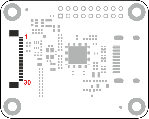
| FPC30 connector pin | Function name | Description |
|---|---|---|
| 1 | GND | - |
| 2 | - | - |
| 3 | HPD | HPD line from HDMI (voltage translated to 3.3V) |
| 4 | +5V | Power supply (input) |
| 5 | +5V | Power supply (input) |
| 6 | +3.3V | Power supply (input) |
| 7 | +3.3V | Power supply (input) |
| 8 | GND | - |
| 9 | SPDIF-TX | SPDIF input from SBC |
| 10 | INT | Interrupt output (voltage translated to 3.3V) |
| 11 | RESET | Reset input (voltage translated to 3.3V) |
| 12 | GND | - |
| 13 | SDA | I2C SDA line (voltage translated to 3.3V) |
| 14 | SCL | I2C SCL line (voltage translated to 3.3V) |
| 15 | GND | - |
| 16 | D3n | MIPI-DSI lane 3 negative line |
| 17 | D3p | MIPI-DSI lane 3 positive line |
| 18 | GND | - |
| 19 | D2n | MIPI-DSI lane 2 negative line |
| 20 | D2p | MIPI-DSI lane 2 positive line |
| 21 | GND | - |
| 22 | D1n | MIPI-DSI lane 1 negative line |
| 23 | D1p | MIPI-DSI lane 1 positive line |
| 24 | GND | - |
| 25 | D0n | MIPI-DSI lane 0 negative line |
| 26 | D0p | MIPI-DSI lane 0 positive line |
| 27 | GND | - |
| 28 | CLKn | MIPI-DSI clock negative line |
| 29 | CLKp | MIPI-DSI clock positive line |
| 30 | GND | - |
LVDS (output) Pinout
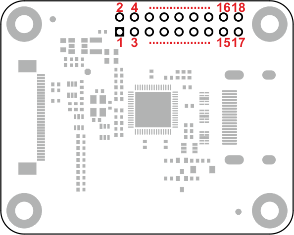
| LVDS connector pin | Function name | Description |
|---|---|---|
| 1 | +5V | Power supply for external devices (max. 20 mA) Internally connected with pin 2 |
| 2 | +5V | Power supply for external devices (max. 20 mA) Internally connected with pin 1 |
| 3 | - | - |
| 4 | GND | - |
| 5 | GND | - |
| 6 | GND | - |
| 7 | D0n | LVDS D0n data line |
| 8 | D0p | LVDS D0p data line |
| 9 | D1n | LVDS D1n data line |
| 10 | D1p | LVDS D1p data line |
| 11 | D2n | LVDS D2n data line |
| 12 | D2p | LVDS D2p data line |
| 13 | GND | - |
| 14 | GND | - |
| 15 | CLKn | LVDS CLKn clock line |
| 16 | CLKp | LVDS CLKp clock line |
| 17 | D3p | LVDS D3p data line |
| 18 | D3n | LVDS D3n data line |
HDMI (output) Pinout

Dimensions
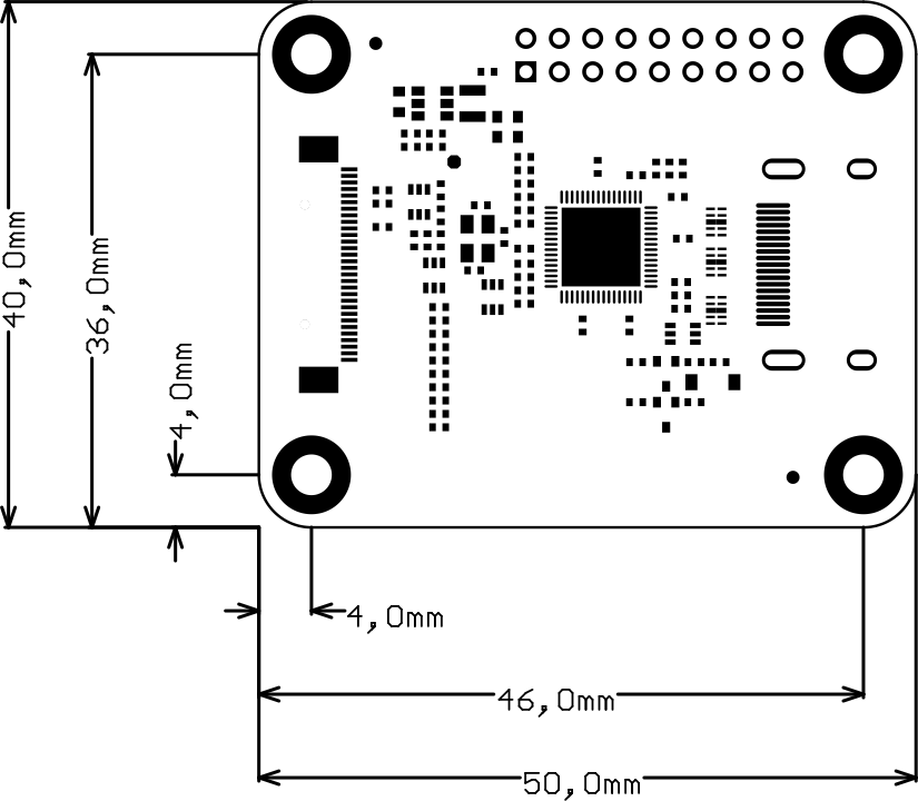
| LVDS connector pin | Function name | Description |
|---|