StarSOM-STM32H757 Datasheet and Pinout
From SomLabs Wiki

StarSOM-STM32H757 Datasheet and Pinout
General description
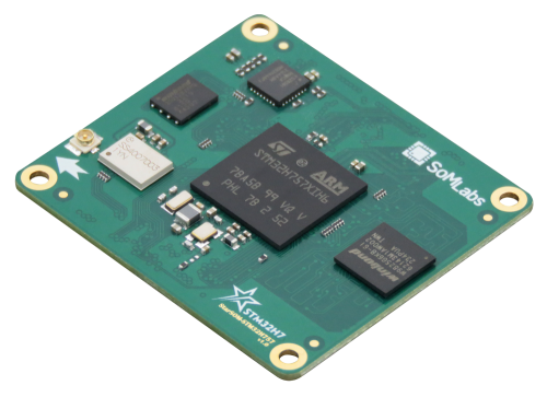
The StarSOM-STM32H757 family is a small size and low profile SoM based on the STMIcroelectronics dual-core MCU, which features an advanced implementation of a ARM Cortex-M7 (up to @480MHz) and Cortex-M4 (up to @240MHz) cores.
The StarSOM-STM32H757 is a low power highly integrated SoM (System on Module) featuring high computation power, on-board Ethernet PHY 10/100, 802.11b/g/n Wi-Fi and Bluetooth v5.1 connectivity. The option of integrated, fully certified Wi-Fi and Bluetooth module simplifies the carrier board design and is ideally suited for wireless application. The StarSOM-STM32H757 provides a variety internal and external memory configurations, including flexible range of SDRAM, and QSPI Flash that meets our customers requirements.
The SoM supports connections to a variety of interfaces: two high-speed USB on-the-go with PHY, dual Ethernet (single PHY on-board), audio, display with touch panel and serial interfaces. In addition, the system supports industrial grade targeting embedded application.
SoMLabs also provides a complete hardware and software development board for the SoM in the form of a carrier board and optional TFT display and touch panel.
Applications
- Industrial embedded real-time computer
- Home Appliances
- Home Automation – Smart Home
- Human-machine Interfaces (HMI)
- Point-of-sales (POS) terminals
- Cash Register
- 2D barcode scanners and printers
- Smart grid infrastructure
- IoT gateways
- Residential gateways
- Machine vision equipment
- Robotics
- Fitness/outdoor equipment
Features
- Powered by ST STM32H757 advanced MCU
- Core clock up to 480 (Cortex-M7)/240 MHz (Cortex-M4)
- Up to 32MB SDRAM
- Up to 32MB QSPI Flash
- Optional Murata 802.11b/g/n Wi-Fi and Bluetooth v5.1 module
- Power-efficient and cost-optimized solution
- Ideal for industrial IoT and embedded applications
- Integrated security features
Pictures of SOM versions
| Version | Photo |
|---|---|
| QSPI and WiFi/BLE on-board |
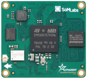 |
| Wi-Fi and Ethernet PHY10/100 are available as an options. |
Ordering info
| SLS | Product type SLS - System on Module |
| N | SOM Name 0 - StarSOM |
| H757 | CPU Family 5 - STM32H757XI |
| CpuType | CPU Type H757 - Dual core STM32H757XI |
| Clock | CPU Clock Speed 480C - Cortex-M7 @480MHz/Cortex-M4 @240MHz |
| RamSize | SDRAM Size 0R - No external SDRAM 32R - 32MB |
| FlashSize | QSPI Flash Size 0QSPI - no external Flash 4QSPI - 4MB QSPI Flash 16QSPI - 16MB QSPI Flash 32QSPI - 32MB QSPI Flash |
| SF | Special Features 0SF - No Special Features 1WB - Built-in Murata 802.11b/g/n WiFI/BLE5.1 2ET - Built-in Microchip 100Mb Ethernet PHY 3WE - Built-in Murata 802.11b/g/n WiFI/BLE5.1 and Microchip 100Mb Ethernet PHY |
| TEMP | Operating Temperature E - Extended: -30 to +70 C I - Industrial: -40 to +85 C |
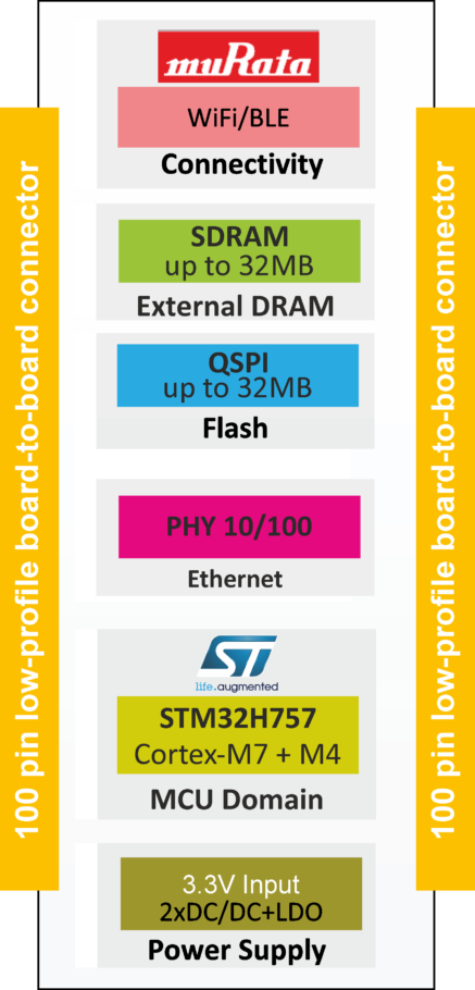
Block Diagram
Operating ranges
| Parameter | Value | Unit | Comment |
|---|---|---|---|
| Power Supply | Connected to +3V3IN pins | ||
| Input GPIO voltage | - | ||
| Environment temperature1 | oC | Industrial range w/o WiFi module | |
| Industrial range with WiFi module | |||
| Consumer range |
Note:
1. Maximum MCU junction temperature is +125oC.
Electrical parameters
| SOM signal name |
Parameter | Value | Units | ||
|---|---|---|---|---|---|
| Min. | Typ. | Max. | |||
| VDD-3V3 | Supply Voltage | 3.15 | 3.3 | 3.45 | V |
| IVDD-3V3 | Total Supply Current | - | 115 | 785 | mA |
| VGPIO (TT_xx) | GPIO Input Voltage | 0 | 3.3 | 3.6 | V |
| VGPIO (except TT_xx) | GPIO Input Voltage | 0 | 3.3 | 5.5 | V |
| VBAT | SNVS Backup Battery Supply |
1.2 | - | 3.6 | V |
| VDDA | ADC Inputs Voltage | 0 | - | 3.6 | V |
Note:
1. VDD50USB and VDD33USB power input are connected to VDD-3V3.
2. VDDA and VREF+ are connected to VDD-3V3.
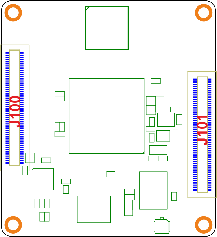
SOM pinout
StarSOM-STM32H757 board-to-board connectors view (top view)
StarSOM-STM32H757 connectors type: Hirose DF40C100DP04V51
| SoM pin number | Default function | GPIO | TFBGA265 ball | Notes |
|---|---|---|---|---|
| J100 | ||||
| 1 | GND | - | - | |
| 2 | GND | - | - | |
| 3 | USB2.VBUS | PB13 | U14 | |
| 4 | DSI.CK_P | DSI_CKP | L16 | MIPI-DSI display interface line |
| 5 | USB2.D_N | PB14 | U15 | USB transceiver line |
| 6 | DSI.CK_N | DSI_CKN | L17 | MIPI-DSI display interface line |
| 7 | USB2.D_P | PB15 | T15 | USB transceiver line |
| 8 | GND | - | - | |
| 9 | GND | - | - | |
| 10 | DSI.D0_P | DSI_D0P | M16 | MIPI-DSI display interface line |
| 11 | USB2.ID | PB12 | T14 | |
| 12 | DSI.D0_N | DSI_D0N | M17 | MIPI-DSI display interface line |
| 13 | PORTB.1 | PB1 | T5 | |
| 14 | GND | - | - | |
| 15 | - | - | - | |
| 16 | DSI.D1_P | DSI_D1P | K16 | MIPI-DSI display interface line |
| 17 | - | - | - | |
| 18 | DSI.D1_N | DSI_D1N | K17 | MIPI-DSI display interface line |
| 19 | - | - | - | |
| 20 | GND | - | - | |
| 21 | - | - | - | |
| 22 | PORTB.0 | PB0 | U5 | |
| 23 | - | - | - | |
| 24 | I2C3.SDA | PH8 | T13 | |
| 25 | - | - | - | |
| 26 | I2C3.SCL | PH7 | U13 | |
| 27 | - | - | - | |
| 28 | PORTH.6 | PH6 | T11 | |
| 29 | - | - | - | |
| 30 | PORTB.11 | PB11 | P12 | |
| 31 | GND | - | - | |
| 32 | PORTH.11 | PH11 | R14 | |
| 33 | PORTB.2 | PB2 | R6 | |
| 34 | PORTB.10 | PB10 | P11 | |
| 35 | USB1.VBUS | PA9 | D15 | |
| 36 | LCD.CLK | PG7 | F16 | |
| 37 | USB1.D_N | PA11 | E17 | USB transceiver line |
| 38 | GND | - | - | |
| 39 | USB1.D_P | PA12 | E16 | USB transceiver line |
| 40 | LCD.VSYNC | PI13 | H2 | |
| 41 | GND | - | - | |
| 42 | LCD.HSYNC | PI12 | H1 | |
| 43 | USB1.ID | PA10 | D14 | |
| 44 | LCD.DE | PK7 | D7 | |
| 45 | - | - | - | |
| 46 | GND | - | - | |
| 47 | - | - | - | |
| 48 | LCD.R7 | PJ6 | N15 | |
| 49 | - | - | - | |
| 50 | LCD.R6 | PJ5 | R12 | |
| 51 | - | - | - | |
| 52 | LCD.R5 | PJ4 | U7 | |
| 53 | - | - | - | |
| 54 | LCD.R4 | PJ3 | U6 | |
| 55 | - | - | - | |
| 56 | LCD.R3 | PJ2 | T6 | |
| 57 | GND | - | - | |
| 58 | LCD.R2 | PJ1 | P6 | |
| 59 | LED0 | - | - | LED0/nWAYEN of KSZ8081RNBCA (on-board Ethernet PHY) |
| 60 | LCD.R1 | PJ0 | N6 | |
| 61 | LED1 | - | - | LED1/SPEED of KSZ8081RNBCA (on-board Ethernet PHY) |
| 62 | LCD.R0 | PI15 | P5 | |
| 63 | GND | - | - | |
| 64 | GND | - | - | |
| 65 | ETH.TX_P | - | - | TXP output of KSZ8081RNBCA (on-board Ethernet PHY) |
| 66 | LCD.G7 | PK2 | H17 | |
| 67 | ETH.TX_N | - | - | TXN output of KSZ8081RNBCA (on-board Ethernet PHY) |
| 68 | LCD.G6 | PK1 | J15 | |
| 69 | GND | - | - | |
| 70 | LCD.G5 | PK0 | J14 | |
| 71 | ETH.RX_P | - | - | RXP input of KSZ8081RNBCA (on-board Ethernet PHY) |
| 72 | LCD.G4 | PJ11 | K14 | |
| 73 | ETH.RX_N | - | - | RXN input of KSZ8081RNBCA (on-board Ethernet PHY) |
| 74 | LCD.G3 | PJ10 | L14 | |
| 75 | GND | - | - | |
| 76 | LCD.G2 | PJ9 | M14 | |
| 77 | GND | - | - | |
| 78 | LCD.G1 | PJ8 | N13 | |
| 79 | GND | - | - | |
| 80 | LCD.G0 | PJ7 | N14 | |
| 81 | VDD-3V3 | - | - | External power supply |
| 82 | GND | - | - | |
| 83 | VDD-3V3 | - | - | External power supply |
| 84 | LCD.B7 | PK6 | C7 | |
| 85 | VDD-3V3 | - | - | External power supply |
| 86 | LCD.B6 | PK5 | A8 | |
| 87 | VDD-3V3 | - | - | External power supply |
| 88 | LCD.B5 | PK4 | B8 | |
| 89 | VDD-3V3 | - | - | External power supply |
| 90 | LCD.B4 | PK3 | C8 | |
| 91 | VDD-3V3 | - | - | External power supply |
| 92 | LCD.B3 | PJ15 | B10 | |
| 93 | VDD-3V3 | - | - | External power supply |
| 94 | LCD.B2 | PJ14 | D10 | |
| 95 | VDD-3V3 | - | - | External power supply |
| 96 | LCD.B1 | PJ13 | E10 | |
| 97 | VDD-3V3 | - | - | External power supply |
| 98 | LCD.B0 | PJ12 | D11 | |
| 99 | VDD-3V3 | - | - | External power supply |
| 100 | GND | - | - | |
| J101 | ||||
| 1 | GND | - | - | |
| 2 | GND | - | - | |
| 3 | PA1_C | PA1_C | T2 | |
| 4 | RECOVERY | If "RECOVERY"=0 then BOOT0=1 (pin E8) Leave open for normal boot | ||
| 5 | PA0_C | PA0_C | T1 | |
| 6 | - | - | - | |
| 7 | PC3_C | PC3_C | R2 | |
| 8 | RESET | nRST | K1 | Reset input |
| 9 | PC2_C | PC2_C | R1 | |
| 10 | GND | - | - | |
| 11 | GND | - | - | |
| 12 | - | - | - | |
| 13 | PORTA.0 | PA0 | N5 | |
| 14 | - | - | - | |
| 15 | PORTA.5 | PA5 | T3 | |
| 16 | GND | - | - | |
| 17 | PORTH.5 | PH5 | P4 | |
| 18 | UART7.CTS | PF9 | L4 | |
| 19 | PORTH.4 | PH4 | P3 | |
| 20 | UART7.RTS | PF8 | K4 | |
| 21 | PORTH.3 | PH3 | P2 | |
| 22 | UART7.RXD | PF6 | K2 | |
| 23 | PORTH.2 | PH2 | N2 | |
| 24 | UART7.TXD | PF7 | K3 | |
| 25 | PORTI.11 | PI11 | F4 | |
| 26 | GND | - | - | |
| 27 | PORTE.6 | PE6 | E5 | |
| 28 | PDR-ON | PDR-ON | E7 | Internally pulled-up with 10kOhm |
| 29 | - | - | - | |
| 30 | GND | - | - | |
| 31 | - | - | - | |
| 32 | - | - | - | |
| 33 | GND | - | - | |
| 34 | - | - | - | |
| 35 | I2C1.SCL | PB8 | D5 | |
| 36 | PORTH.9 | PH9 | R13 | |
| 37 | I2C1.SDA | PB9 | D4 | |
| 38 | PORTH.10 | PH10 | P13 | |
| 39 | PORTE.5 | PE5 | D1 | |
| 40 | PORTG.10 | PG10 | A9 | |
| 41 | PORTE.3 | PE3 | D3 | |
| 42 | PORTH.12 | PH12 | R14 | |
| 43 | USART1.RXD | PB7 | C5 | |
| 44 | PORTE.4 | PE4 | D2 | |
| 45 | USART1.TXD | PB6 | B5 | |
| 46 | PORTI.4 | PI4 | A4 | |
| 47 | - | - | - | |
| 48 | PORTI.6 | PI6 | A2 | |
| 49 | - | - | - | |
| 50 | PORTI.7 | PI7 | B3 | |
| 51 | - | - | - | |
| 52 | PORTA.6 | PA6 | R3 | |
| 53 | PORTB.5 | PB5 | A5 | |
| 54 | PORTA.4 | PA4 | U3 | |
| 55 | PORTD.7 | PD7 | C11 | |
| 56 | PORTI.5 | PI5 | A3 | |
| 57 | PORTG.14 | PG14 | D8 | |
| 58 | GND | - | - | |
| 59 | PORTG.9 | PG9 | A10 | |
| 60 | VBAT | VBAT | B1 | |
| 61 | CAN1.RX | PH14 | B17 | |
| 62 | GND | - | - | |
| 63 | CAN1.TX | PH13 | D16 | |
| 64 | JTAG.TCK | PA14 | B14 | SWCLK interface |
| 65 | GND | - | - | |
| 66 | JTAG.TDI | PA15 | A14 | |
| 67 | PORTI.101 | PI10 | F3 | Shared with BT-HWAKE (1DX) Used by WiFi/BLE 1DX module if installed |
| 68 | JTAG.TDO | PB3 | C6 | |
| 69 | PORTI.91 | PI9 | E2 | Shared with BT-WAKE (1DX) Used by WiFi/BLE 1DX module if installed |
| 70 | JTAG.TMS | PA13 | C15 | SWDIO interface |
| 71 | PORTI.81 | PI8 | E4 | Shared with BT-EN (1DX) Used by WiFi/BLE 1DX module if installed |
| 72 | JTAG.TRST | PB4 | B7 | |
| 73 | PORTI.141 | PI14 | H3 | Shared with WLAN-HWAKE (1DX) Used by WiFi/BLE 1DX module if installed |
| 74 | GND | - | - | |
| 75 | PORTC.71 | PC7 | F13 | Shared with WLAN-EN (1DX) Used by WiFi/BLE 1DX module if installed |
| 76 | - | - | - | |
| 77 | UART2X.CTS1 | PD3 | B12 | Shared with WLAN-EN (1DX) Used by WiFi/BLE 1DX module if installed |
| 78 | - | - | - | |
| 79 | UART2X.RTS1 | PD4 | A12 | Shared with WLAN-EN (1DX) Used by WiFi/BLE 1DX module if installed |
| 80 | - | - | - | |
| 81 | UART2X.RXD1 | PD6 | B11 | Shared with WLAN-EN (1DX) Used by WiFi/BLE 1DX module if installed |
| 82 | - | - | - | |
| 83 | UART2X.TXD1 | PD5 | A11 | Shared with WLAN-EN (1DX) Used by WiFi/BLE 1DX module if installed |
| 84 | - | - | - | |
| 85 | GND | - | - | |
| 86 | GND | - | - | |
| 87 | SDMMC1X.D11 | PC9 | E14 | SDMMC1.D1 line separated from SDMMC1X.D1 with 0 Ohm Used by WiFi/BLE 1DX module if installed |
| 88 | I2S2.WS | PI0 | A16 | |
| 89 | SDMMC1X.D01 | PC8 | E13 | SDMMC1.D0 line separated from SDMMC1X.D0 with 0 Ohm Used by WiFi/BLE 1DX module if installed |
| 90 | I2S2.CK | PI1 | A15 | |
| 91 | SDMMC1X.CK1 | PC12 | C12 | SDMMC1.CK line separated from SDMMC1X.CK with 0 Ohm Used by WiFi/BLE 1DX module if installed |
| 92 | I2S2.SDI | PI2 | B15 | |
| 93 | SDMMC1X.CMD1 | PD2 | D12 | SDMMC1.CMD line separated from SDMMC1X.CMD with 0 Ohm Used by WiFi/BLE 1DX module if installed |
| 94 | I2S2.SDO | PI3 | C14 | |
| 95 | SDMMC1X.D31 | PC11 | B13 | SDMMC1.D1 line separated from SDMMC1X.D3 with 0 Ohm Used by WiFi/BLE 1DX module if installed |
| 96 | GND | - | - | |
| 97 | SDMMC1X.D21 | PC10 | A13 | SDMMC1.D1 line separated from SDMMC1X.D2 with 0 Ohm Used by WiFi/BLE 1DX module if installed |
| 98 | I2S2.MCK | PC6 | F14 | |
| 99 | GND | - | - | |
| 100 | GND | - | - | |
| Internal system connections | ||||
| - | PC14-OSC32_IN | C2 | 32 kHz crystal connected | |
| - | PC14-OSC32_OUT | C1 | 32 kHz crystal connected | |
| QSPI.NCS | PG6 | G15 | On-board QSPI Flash memory | |
| QSPI.CLK | PF10 | L3 | ||
| QSPI.IO0 | PD11 | R15 | ||
| QSPI.IO1 | PD12 | R16 | ||
| QSPI.IO2 | PE2 | C3 | ||
| QSPI.IO3 | PD13 | R17 | ||
| DRAM.CKE | PC3 | M4 | On-board SDRAM memory | |
| DRAM.CLK | PG8 | F15 | ||
| DRAM.DM0 | PE0 | C4 | ||
| DRAM.DM1 | PE1 | B4 | ||
| DRAM.CS0 | PC2 | M3 | ||
| DRAM.WE | PC0 | L2 | ||
| DRAM.CAS | PG15 | D6 | ||
| DRAM.RAS | PF11 | T7 | ||
| DRAM.BA0 | PG4 | H14 | ||
| DRAM.BA1 | PG5 | G15 | ||
| DRAM.A0 | PF0 | G4 | ||
| DRAM.A1 | PF1 | G3 | ||
| DRAM.A2 | PF2 | G15 | ||
| DRAM.A3 | PF3 | H4 | ||
| DRAM.A4 | PF4 | J5 | ||
| DRAM.A5 | PF5 | J4 | ||
| DRAM.A6 | PF12 | R7 | ||
| DRAM.A7 | PF13 | P7 | ||
| DRAM.A8 | PF14 | P8 | ||
| DRAM.A9 | PF15 | R9 | ||
| DRAM.A10 | PG0 | T8 | ||
| DRAM.A11 | PG1 | U8 | ||
| DRAM.A12 | PG2 | H16 | ||
| DRAM.D0 | PD14 | P16 | ||
| DRAM.D1 | PD15 | P15 | ||
| DRAM.D2 | PD0 | D13 | ||
| DRAM.D3 | PD1 | E12 | ||
| DRAM.D4 | PE7 | U9 | ||
| DRAM.D5 | PE8 | T9 | ||
| DRAM.D6 | PE9 | P9 | ||
| DRAM.D7 | PE10 | N9 | ||
| DRAM.D8 | PE11 | P10 | ||
| DRAM.D9 | PE12 | R10 | ||
| DRAM.D10 | PE13 | T10 | ||
| DRAM.D11 | PE14 | U10 | ||
| DRAM.D12 | PE15 | R11 | ||
| DRAM.D13 | PD8 | U16 | ||
| DRAM.D14 | PD9 | T17 | ||
| DRAM.D15 | PD10 | T16 | ||
| ENET.MDIO | PA2 | N3 | On-board Ethernet PHY | |
| ENET.MDC | PC1 | M2 | ||
| ENET.RXD0 | PC4 | T4 | ||
| ENET.RXD1 | PC5 | U4 | ||
| ENET.CRS-DV | PA7 | R5 | ||
| ENET.REF-CLK | PA1 | N4 | ||
| ENET.TXD0 | PG13 | D9 | ||
| ENET.TXD1 | PG12 | C9 | ||
| ENET.TXEN | PG11 | B9 | ||
| ENET.INT | PG3 | H15 | ||
| ENET.RST | PH15 | B16 | ||
| CLK-25MHz | PA8 | E15 | ||
| WLAN-EN1 | PC7 | F13 | On-board WiF/BLE module | |
| WLAN-HWAKE1 | PI14 | H3 | ||
| SDMMC1.CK1 | PC12 | C12 | ||
| SDMMC1.CMD1 | PD2 | D12 | ||
| SDMMC1.D01 | PC8 | E13 | ||
| SDMMC1.D11 | PC9 | E14 | ||
| SDMMC1.D21 | PC10 | A13 | ||
| SDMMC1.D31 | PC11 | B13 | ||
| CLK-32KHz | PA3 | U2 | ||
| BT-WAKE1 | PI9 | E2 | ||
| BT-HWAKE1 | PI10 | F3 | ||
| BT-EN1 | PI8 | E4 | ||
| UART2.CTS1 | PD3 | B12 | ||
| UART2.RTS1 | PD4 | A12 | ||
| UART2.RXD1 | PD6 | B11 | ||
| UART2.TXD1 | PD5 | A11 | ||
Note:
1. Dual use pins: if 1DX (WiFi/BLE) module is installed on the StarSOM-STM32H757 module these pins are not available for user.
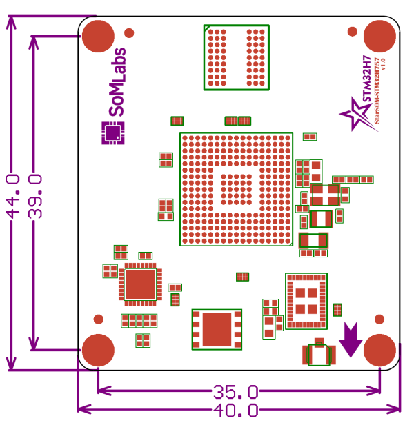
Dimensions
