VisionCB-6ULL-IND-HDMI v.1.0 Datasheet and Pinout
From SomLabs Wiki

VisionCB-6ULL-IND-HDMI Datasheet and Pinout
General description

VisionCB-6ULL-IND-HDMI is a carrier board for the VisionSOM family of computer-on-modules which are powered by NXP i.MX 6UL or i.MX 6ULL application processors (ARM Cortex-A7). A carrier board, together with a System on Module (SoM), makes a complete development platform similar to SBC. The carrier board houses the most common interfaces such as HDMI video output, USB, Ethernet, additional microSD socket, etc. A large variety of interfaces allows to use it as both a complete development platform or as a stand-alone end-product.
The carrier board connects with the SoM via a standard SODIMM connector.
Applications
- Industrial embedded Linux computer
- Home Appliances
- Home Automation – Smart Home
- Human-machine Interfaces (HMI)
- Point-of-sales (POS) terminals
- Cash Register
- 2D barcode scanners and printers
- Smart grid Infrastructure
- IoT gateways
- Residential getaways
- Machine vision equipment
- Robotics
- Fitness/outdoor equipment
Features
- Industrial grade Carrier Board (Base Board) compatible with the VisionSOM family of modules based on NXP i.MX 6UL / 6ULL application processors
- Core clock up to 696MHz (VisionSOM-6UL) or up to 900MHz (VisionSOM-6ULL)
- Up to 512MB SDRAM DDR3L (depends on used VisionSOM module)
- Up to 512MB NAND Flash / 32GB eMMC / uSD memory card (depends on used VisionSOM module)
- Optional Murata 802.11b/g/n Wi-Fi and Bluetooth v4.1+EDR module
- SoM Interface: SODIMM200
- Expansion Connectors:
- 2x25 Pin Headers (Female)
- microSD Card socket
- Communication Connectors:
- 1x Ethernet 10/100Mbit/s, RJ45
- 2x USB Host Type A connectors
- 1x USB OTG Micro AB connector
- Display Interface: HDMI Connector (1366 x 768 Max. Resolution)
- Embedded Real-Time Clock (RTC) with back-up battery option (CR1220 battery needed)
- Power Supply
- Terminal block connector: Input Voltage 9-12V DC
- Temperature Range: 0 to +70°C
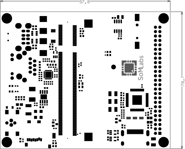
- Board Size: 98mm x 79mm x 22mm
Pictures of VisionCB-6ULL-IND-HDMI board
| Version | Photo |
|---|---|
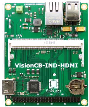
| VisionCB-6ULL-IND-HDMI board only |
 |
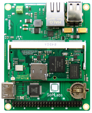
| VisionCB-6ULL-IND-HDMI board with VisionSOM-6ULL |
 |
Ordering info
VisionCB-6ULL-IND-HDMI v.1.0
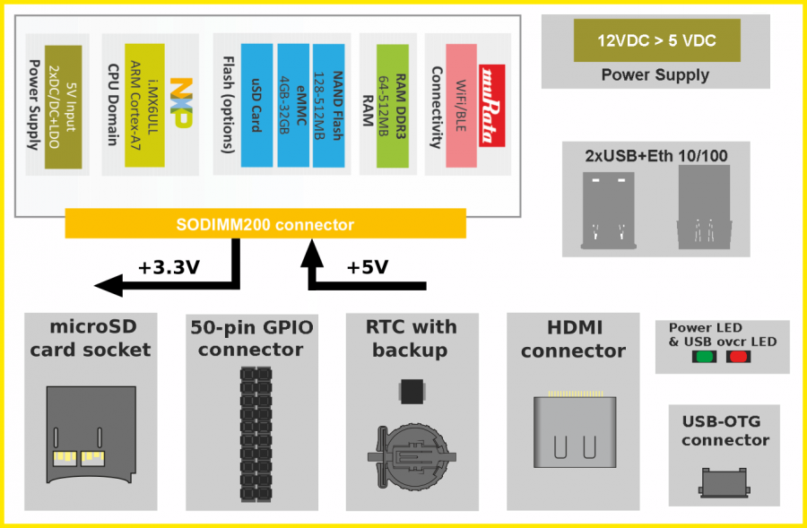
Block Diagram
Electrical parameters
| Parameter | Value | Units | Comment | ||
|---|---|---|---|---|---|
| Min. | Typ. | Max. | |||
| Power Supply (Con100 input) | 9.0 | 12.0 | 15.0 | V | Polarized terminal block connector |
| Supply current | - | - | 0.15 | A | Excluding LCD, USB and antoher external loads |
| Output GPIO voltage (Con1) | 0 | - | 3.3 | V | GPIO connector (current limited; max <250mA [RMS]) |
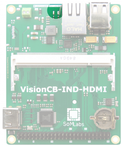
Onboard LEDs
| LED | Color | Description |
|---|---|---|
| LED100 (PWR) | Green | Power indicator |
| LED200 (USB OVR) | Red | USB Overcurrent indicator |
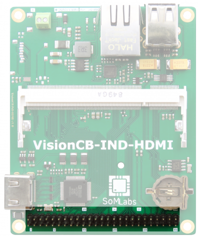
2x25 pin header
| J504 Pin | Default function name | Description |
|---|---|---|
| 1 | CSI-HSYNC | Video CMOS sensor signal or universal GPIO with 3.3V logic levels. |
| 2 | CSI-VSYNC | Video CMOS sensor signal or universal GPIO with 3.3V logic levels. |
| 3 | CSI-DATA0 | Video CMOS sensor signal or universal GPIO with 3.3V logic levels. |
| 4 | CSI-DATA2 | Video CMOS sensor signal or universal GPIO with 3.3V logic levels. |
| 5 | CSI-DATA1 | Video CMOS sensor signal or universal GPIO with 3.3V logic levels. |
| 6 | CSI-DATA3 | Video CMOS sensor signal or universal GPIO with 3.3V logic levels. |
| 7 | CSI-DATA4 | Video CMOS sensor signal or universal GPIO with 3.3V logic levels. |
| 8 | CSI-DATA5 | Video CMOS sensor signal or universal GPIO with 3.3V logic levels. |
| 9 | CSI-MCLK | Video CMOS sensor signal or universal GPIO with 3.3V logic levels. |
| 10 | CSI-DATA7 | Video CMOS sensor signal or universal GPIO with 3.3V logic levels. |
| 11 | CSI_PIXCLK | Video CMOS sensor signal or universal GPIO with 3.3V logic levels. |
| 12 | CSI-DATA6 | Video CMOS sensor signal or universal GPIO with 3.3V logic levels. |
| 13 | ENET2_TXD0 | Default: ENET2 TXD0 line or universal GPIO with 3.3V logic levels. |
| 14 | UART3-RTS | Default: UART3 RTS line or universal GPIO with 3.3V logic levels. |
| 15 | ENET2_TXEN | Default: ENET2 TXEN line or universal GPIO with 3.3V logic levels. |
| 16 | UART2-RTS | Default: UART2 RTS line or universal GPIO with 3.3V logic levels. |
| 17 | ENET2_CRS_DV | Default: ENET2 CRS_DV line or universal GPIO with 3.3V logic levels. |
| 18 | UART3-CTS | Default: UART3 CTS line or universal GPIO with 3.3V logic levels. |
| 19 | ENET2_RXD1 | Default: ENET2 RXD1 line or universal GPIO with 3.3V logic levels. |
| 20 | UART1-RTS | Default: UART1 RTS line or universal GPIO with 3.3V logic levels. |
| 21 | ENET2_RXER | Default: ENET2 RXER line or universal GPIO with 3.3V logic levels. |
| 22 | UART2-CTS | Default: UART2 CTS line or universal GPIO with 3.3V logic levels. |
| 23 | ENET2_TX_CLK | Default: ENET2 TX_CLK line or universal GPIO with 3.3V logic levels. |
| 24 | UART1-CTS | Default: UART1 CTS line or universal GPIO with 3.3V logic levels. |
| 25 | UART4-RXD | Default: UART4 RXD input or universal GPIO with 3.3V logic levels. |
| 26 | JTAG-TCK | Default: JTAG TCK input or universal GPIO with 3.3V logic levels. |
| 27 | UART4-TXD | Default: UART4 TXD output or universal GPIO with 3.3V logic levels. |
| 28 | JTAG-nTRST | JTAG TRST input line (active L). |
| 29 | UART3-RXD | Default: UART3 RxD input or universal GPIO with 3.3V logic levels. |
| 30 | JTAG-TMS | Default: JTAG TMS output or universal GPIO with 3.3V logic levels. |
| 31 | UART2-RXD | Default: UART2 RXD input or universal GPIO with 3.3V logic levels. |
| 32 | SNVS-TAMPER2 | Tamper input (SNVS power domain) or GPIO 3.3V. |
| 33 | UART2-TXD | Default: UART2 TXD input or universal GPIO with 3.3V logic levels. |
| 34 | SNVS-TAMPER3 | Tamper input (SNVS power domain) or GPIO 3.3V. |
| 35 | UART1-RXD | Default: UART1 RXD input or universal GPIO with 3.3V logic levels. |
| 36 | SNVS-TAMPER4 | Tamper input (SNVS power domain) or GPIO 3.3V. |
| 37 | UART1-TXD | Default: UART1 TXD input or universal GPIO with 3.3V logic levels. |
| 38 | SNVS-TAMPER5 | Tamper input (SNVS power domain) or GPIO 3.3V. |
| 39 | SNVS-TAMPER0 | Tamper input (SNVS power domain) or GPIO 3.3V. |
| 40 | I2C-SCL | Universal GPIO with 3.3V logic levels. |
| 41 | SNVS-TAMPER1 | Tamper input (SNVS power domain) or GPIO 3.3V. |
| 42 | I2C-SDA | Universal GPIO with 3.3V logic levels. |
| 43 | GPIO5 | Default: General purpose pin GPIO5 |
| 44 | JTAG-TDI | Default: JTAG TDI input or universal GPIO with 3.3V logic levels. |
| 45 | GPIO8 | Default: General purpose pin GPIO8 |
| 46 | GPIO9 | Default: General purpose pin GPIO9 |
| 47 | VCC-3V3 | +3.3V generated by internal SOM LDO converter (limited load current, limit: < 250mA [RMS]). |
| 48 | GND | Ground |
| 49 | VCC-3V3 | +3.3V generated by internal SOM LDO converter (limited load current, limit: < 250mA [RMS]). |
| 50 | GND | Ground |
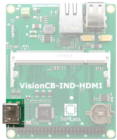
HDMI connector
Dimensions
