VisionCB-iMX93-STD Datasheet and Pinout
From SomLabs Wiki

VisionCB-iMX93-STD Datasheet and Pinout
General description

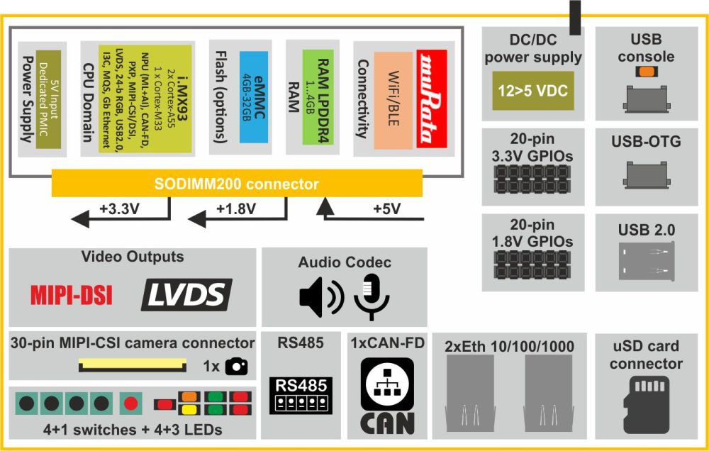
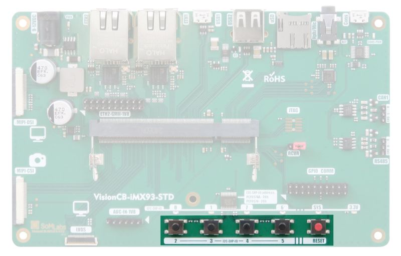
The VisionCB-iMX93-STD (with SOM equipped with heterogenous i.MX935x processor) is a carrier board for the VisionSOM-iMX93family of computer-on-modules which are powered by dual-core NXP MPUs (2 x ARM Cortex-A55 + Cortex-M33). The carrier board, together with a System on Module (SoM), makes a complete development platform similar to SBC. The carrier board houses the most common interfaces such as USB, Ethernet, CAN, RS485, audio codec, etc. A large variety of interfaces allows to use it as both a complete development platform or as a stand-alone end-product. The VisionCB-iMX93-STD is equipped with a simple user interface consisting of 4 buttons and 5 LEDs. VisionCB-iMX93-STD carrier board is also equipped with a large number of popular peripherals, including: RS485, CAN, 10/100/1G Ethernet, MIPI-DSI and camera connectors, serial console port on USB vCOM.
Applications
- Low-cost Gateway
- Domain Controller Compute Off-load Engine
- Human-machine Interfaces (HMI)
- Public Address Systems
- Home Appliances
- Home Automation – Smart Home
- IoT gateways
- Wireless or Networked Speakers
- Residential gateways
- Industrial embedded Linux computer
- Fitness/outdoor equipment
Features
- Carrier Board compatible with the VisionSOM-iMX93 families of modules based on dual core, heterogenous i.MX935x application processors
- SoM Connector: SODIMM200
- Expansion Connectors:
- 3.3V GPIO connector 2x20 Pin Header (Male)
- 1.8V GPIO connector 2x20 Pin Header (Male)
- Communication Connectors:
- 2x Ethernet 10/100/1000Mbit/s (RJ45)
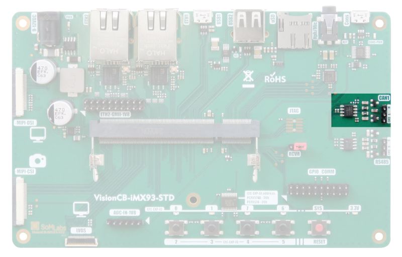
- 1x CAN (1x3 Pin Header, Male)
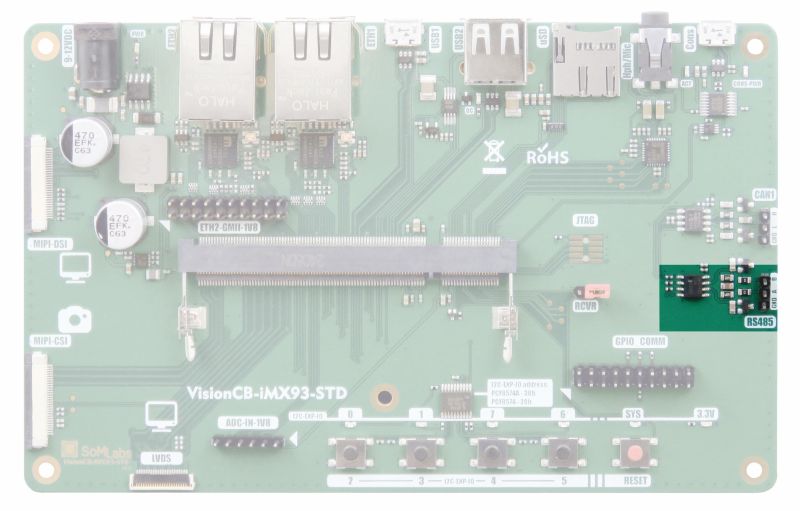
- 1x RS-485 (1x3 Pin Header, Male)
- 1x USB Host Type A connectors
- 1x USB OTG Micro AB connector
- 1x Console MicroUSB B connector
- Audio Interface:
- Mini-jack 3.5mm (headphones + microphone)
- Display Interface:
- 30-pin FFC/FPC MIPI-DSI (up to 4 lanes)
- 22-pin FFC/FPC LVDS (up to 4 lanes)
- Camera Interface:
- 30-pin FFC/FPC MIPI-CSI2 (up to 2 lanes)
- User Interface:
- 4+1 Pushbuttons
- 5+1 LEDs
- External Power Supply 9-12V DC
- Temperature Range: 0 to +70°C
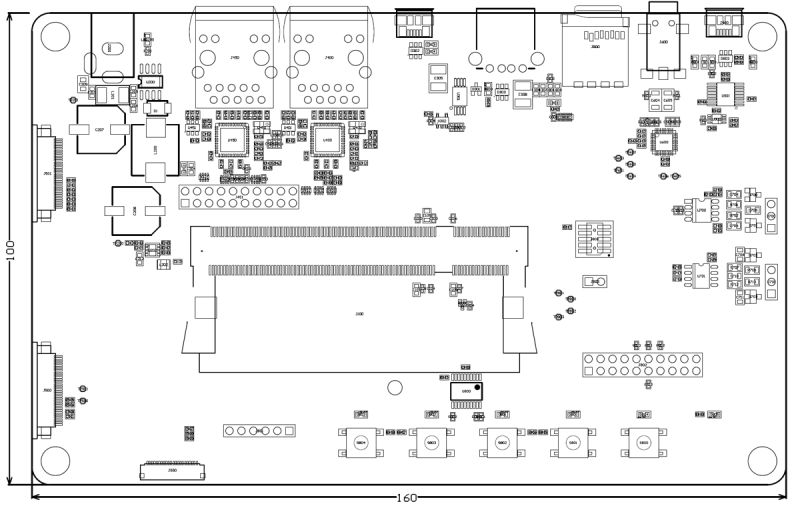
- Board Size: 160mm x 100mm x 20mm
Pictures of VisionCB-iMX93-STD board
| Version | Photo |
|---|---|
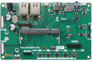
| VisionCB-iMX93-STD board only |
 |
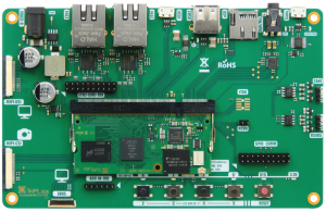
| VisionCB-iMX93-STD with VisionSOM-iMX93 |
 |
Ordering info
Block Diagram
Electrical parameters
| Parameter | Value | Units | Comment | ||
|---|---|---|---|---|---|
| Min. | Typ. | Max. | |||
| Power Supply | 9.0 | 12.0 | 15.0 | V | Positive pole on central connector of J200 |
| Supply current | - | - | 0.21 | A | Excluding LCD, USB and antoher external loads |
| LCD/Camera Power Supply (logic) |
3.25 | 3.3 | 3.35 | V | - |
| LCD/Camera Power Supply (backlight and aux) |
4.75 | 4.87 | 4.95 | V | - |
| 1.8V GPIO voltage | 1.72 | 1.8 | 1.89 | V | - |
| 3.3V GPIO voltage | 3.25 | 3.3 | 3.6 | V | - |
| ADC in voltage | 0 | - | 1.8 | V | On dedicated ADC inputs |
Power supply connector
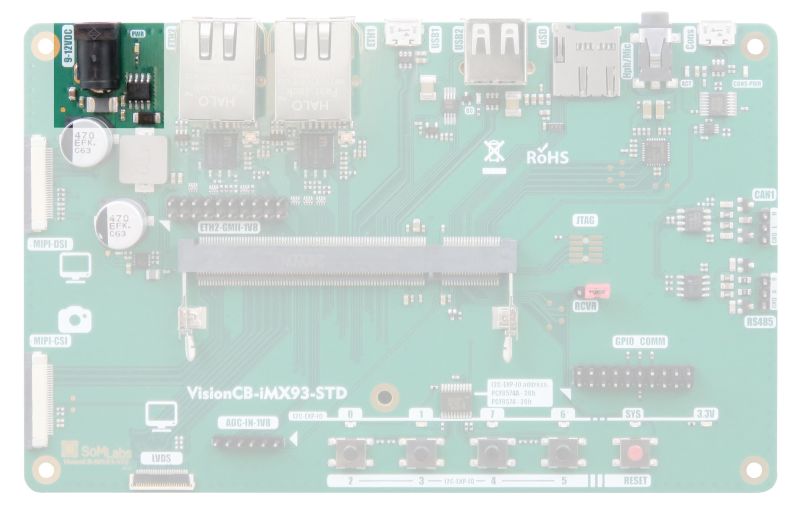
The VisionCB-iMX93-STD is equipped with external power source connector with pin diameter 2.5mm and hole diameter 5mm. The voltage of the external power source should be within the range 9-12 VDC.
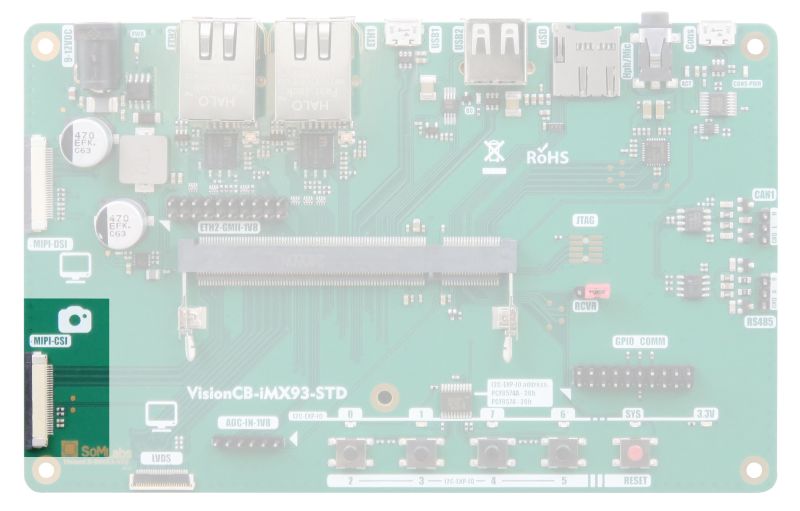
Camera MIPI-CSI interface (FPC/FFC30, 0.5mm)
| Pin | Signal | MPU pin name | Description |
|---|---|---|---|
| 1 | GND | - | - |
| 2 | CSI.CLK_P | MIPI_CSI1_CLK_P | - |
| 3 | CSI.CLK_N | MIPI_CSI1_CLK_N | - |
| 4 | GND | - | - |
| 5 | CSI.DATA0_P | MIPI_CSI1_D0_P | - |
| 6 | CSI.DATA0_N | MIPI_CSI1_D0_N | - |
| 7 | GND | - | - |
| 8 | CSI.DATA1_P | MIPI_CSI1_D1_P | - |
| 9 | CSI.DATA1_N | MIPI_CSI1_D1_N | - |
| 10 | GND | - | - |
| 11 | - | - | - |
| 12 | - | - | - |
| 13 | GND | - | - |
| 14 | - | - | - |
| 15 | - | - | - |
| 16 | GND | - | - |
| 17 | I2C1.SCL | I2C1_SCL | Camera confguration I2C interface (3.3V), shared on SOM with PCA9451AHN PMIC |
| 18 | I2C1.SDA | I2C1_SDA | Camera confguration I2C interface (3.3V), shared on SOM with PCA9451AHN PMIC |
| 19 | GND | - | - |
| 20 | CAM_RST | GPIO2_IO18 | Auxiliary GPIO VisionSOM-iMX93 pin name SPI5.CS0 |
| 21 | CAM_PWER_EN | GPIO2_IO19 | Auxiliary GPIO VisionSOM-iMX93 pin name SPI5.MISO |
| 22 | - | - | - |
| 23 | GND | - | - |
| 24 | +3.3V | - | Power supply for camera module (on both pin: 24 and 25 max. 50 mA) |
| 25 | +3.3V | - | Power supply for camera module (on both pin: 24 and 25 max. 50 mA) |
| 26 | +5V | - | Power supply for camera module (on both pin: 26 and 27 max. 100 mA) |
| 27 | +5V | - | Power supply for camera module (on both pin: 26 and 27 max. 100 mA) |
| 28 | - | - | - |
| 29 | - | - | - |
| 30 | GND | - | - |
Note:
1. The first pin of the MIPI-CSI connector is located in its upper part.
2. Recommended camera module is SL-MIPI-CSI-OV5640
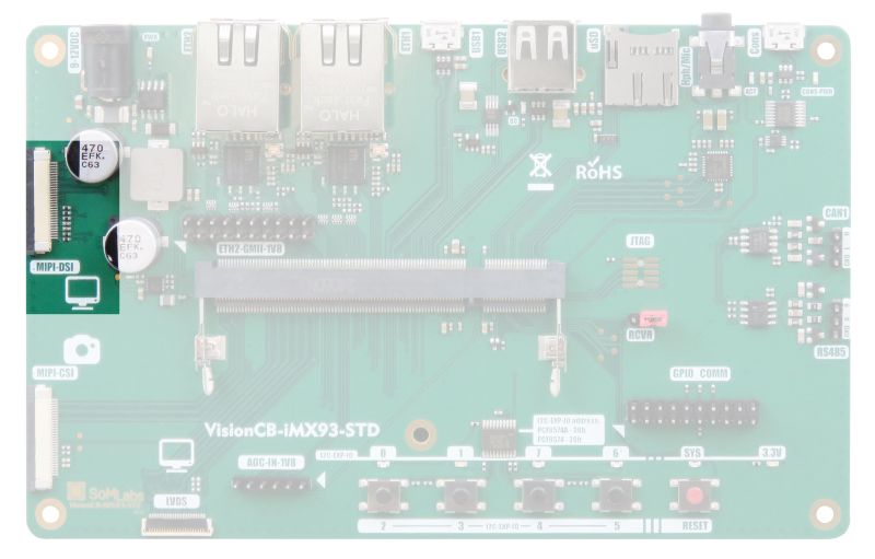
Display MIPI-DSI interface (FPC/FFC30, 0.5mm)
| Pin | Signal | MPU pin name | Description |
|---|---|---|---|
| 1 | GND | - | |
| 2 | DSI.CLK_P | MIPI_DSI1_CLK_P | - |
| 3 | DSI.CLK_N | MIPI_DSI1_CLK_N | - |
| 4 | GND | - | - |
| 5 | DSI.DATA0_P | MIPI_DSI1_D0_P | - |
| 6 | DSI.DATA0_N | MIPI_DSI1_D0_N | - |
| 7 | GND | - | - |
| 8 | DSI.DATA1_P | MIPI_DSI1_D1_P | - |
| 9 | DSI.DATA1_N | MIPI_DSI1_D1_N | - |
| 10 | GND | - | - |
| 11 | DSI.DATA2_P | MIPI_DSI1_D2_P | - |
| 12 | DSI.DATA2_N | MIPI_DSI1_D2_N | - |
| 13 | GND | - | - |
| 14 | DSI.DATA3_P | MIPI_DSI1_D3_P | - |
| 15 | DSI.DATA3_N | MIPI_DSI1_D3_N | - |
| 16 | GND | - | - |
| 17 | I2C1.SCL | I2C1_SCL | Display confguration I2C interface (3.3V), shared on SOM with PCA9451AHN PMIC |
| 18 | I2C1.SDA | I2C1_SDA | Display confguration I2C interface (3.3V), shared on SOM with PCA9451AHN PMIC |
| 19 | GND | - | - |
| 20 | DISP-RST | GPIO2_11 | Optional display reset signal VisionSOM-iMX93 pin name UART7.RTS |
| 21 | TP-INT | GPIO2_IO09 | Optional touch-panel interrupt signal VisionSOM-iMX93 pin name UART7.RXD |
| 22 | TP-RST | GPIO2_IO08 | Optional touch-panel reset signal VisionSOM-iMX93 pin name UART7.TXD |
| 23 | GND | - | - |
| 24 | +3.3V | - | Power supply for display module (on both pins: 21 and 22 max. 50 mA) |
| 25 | +3.3V | - | Power supply for display module (on both pins: 21 and 22 max. 50 mA) |
| 26 | +5V | - | Power supply for display module (on both pins: 21 and 22 max. 200 mA) |
| 27 | +5V | - | Power supply for display module (on both pins: 21 and 22 max. 200 mA) |
| 28 | DSI-BL-PWM | GPIO1_IO07 | Optional PWM backlight signal |
| 29 | DSI-BL-EN | GPIO2_10 | Optional ENABLE backlight signal VisionSOM-iMX93 pin name UART7.CTS |
| 30 | GND | - | - |
Note:
1. The first pin of the MIPI-DSI connector is located in its upper part.
2. Recommended display module for evaluation purposes is SoMLabs SL-TFT7-TP-600-1024-MIPI or similar (connector pinout is fully compatible with this module)
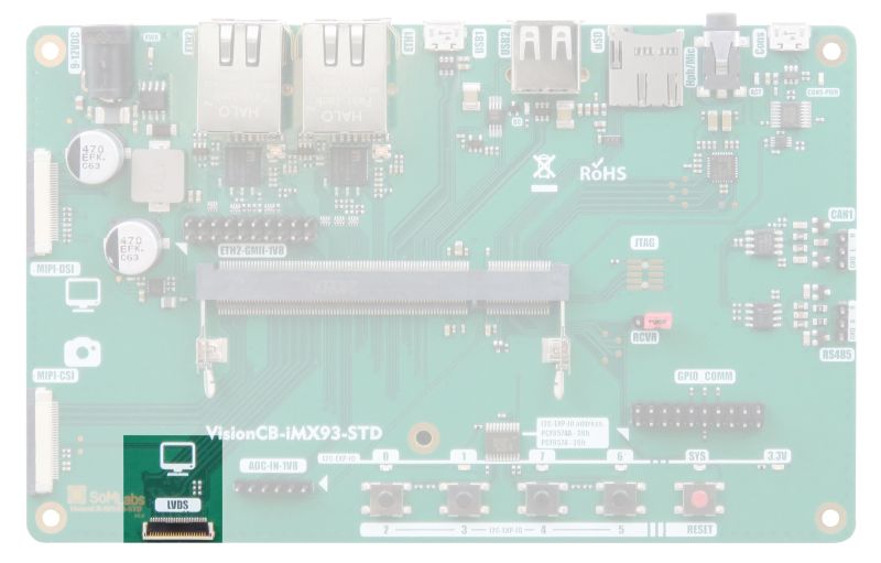
Display LVDS interface (FPC/FFC22, 0.5mm)
| Pin | Signal | MPU pin name | Description |
|---|---|---|---|
| 1 | GND | - | |
| 2 | LVDS.DATA0_N | LVDS_D0_N | - |
| 3 | LVDS.DATA0_P | LVDS_D0_P | - |
| 4 | GND | - | - |
| 5 | LVDS.DATA1_N | LVDS_D1_N | - |
| 6 | LVDS.DATA1_P | LVDS_D1_P | - |
| 7 | GND | - | - |
| 8 | LVDS.DATA2_N | LVDS_D2_N | - |
| 9 | LVDS.DATA2_P | LVDS_D2_P | - |
| 10 | GND | - | - |
| 11 | LVDS.CLK_N | LVDS_CLK_N | - |
| 12 | LVDS.CLK_P | LVDS_CLK_P | - |
| 13 | GND | - | - |
| 14 | LVDS.DATA3_N | LVDS_D3_N | - |
| 15 | LVDS.DATA3_P | LVDS_D3_P | - |
| 16 | PWR_EN | - | Not connected by default, can be connected to SPI5.MOSI |
| 17 | PWM_IN | GPIO2_IO20 | VisionSOM-iMX93 pin name SPI5.MOSI |
| 18 | I2C1.INT | GPIO2_IO21 | Touch panel interrupt SOM pin name SPI5.SCK |
| 19 | I2C1.SCL | I2C1_SCL | Touch panel interface, shared with SOM PMIC (PCA9451AHN) |
| 20 | I2C1.SDA | I2C1_SDA | Touch panel interface, shared with SOM PMIC (PCA9451AHN) |
| 21 | VDD-5V0 | - | Power supply for display module (on both pins: 21 and 22 max. 200 mA) |
| 22 | VDD-5V0 | - | Power supply for display module (on both pins: 21 and 22 max. 200 mA) |
Note:
1. The first pin of the LVDS connector is located on its left side.
2. Recommended display module for evaluation purposes is SoMLabs SL-TFT7-TP-600-1024-LVDS or similar (connector pinout is fully compatible with this module)
USB Console Port
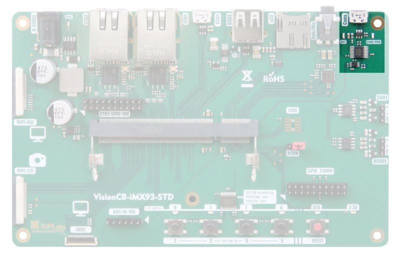
| Console line | MPU signal | MPU pin name |
|---|---|---|
| CONSOLE-TXD | UART1.RXD | UART1_RXD |
| CONSOLE-RXD | UART1.TXD | UART1_TXD |
ADC inputs connector
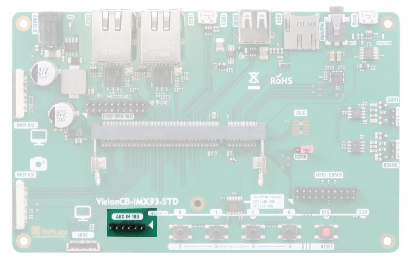
| Pin | Signal | Description |
|---|---|---|
| 1 | GND | - |
| 2 | IN3 | Dedicated 12-bit ADC input 1.8V compatible |
| 3 | IN2 | Dedicated 12-bit ADC input 1.8V compatible |
| 4 | IN1 | Dedicated 12-bit ADC input 1.8V compatible |
| 5 | IN0 | Dedicated 12-bit ADC input 1.8V compatible |
| 6 | VDD-1V8 | - |
1.8V GPIO connector (ETH2-GMII-1V8)
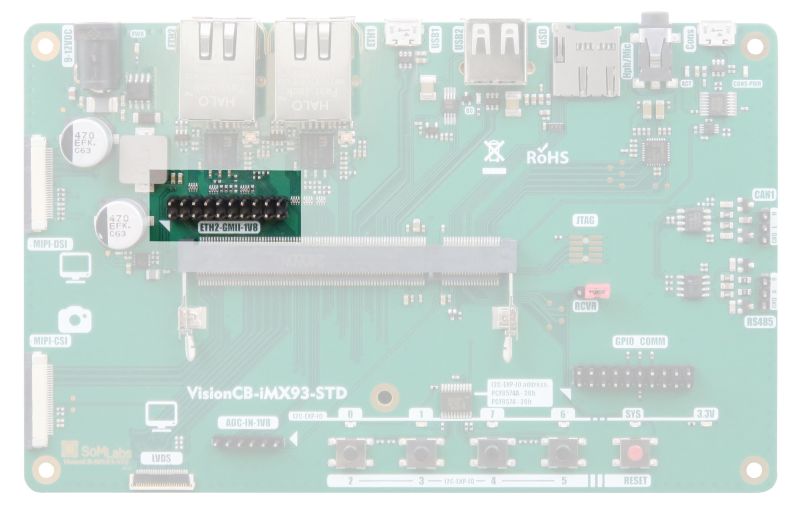
| Pin | Signal | MPU pin name | Description |
|---|---|---|---|
| 1 | 1.8V | - | Reference voltage for external logic |
| 2 | 1.8V | - | Reference voltage for external logic |
| 3 | ENET2.TXD1 | ENET2_TD1 | GMII interface line with optional GPIO functions |
| 4 | ENET2.TXD0 | ENET2_TD0 | GMII interface line with optional GPIO functions |
| 5 | ENET2.TXD3 | ENET2_TD3 | GMII interface line with optional GPIO functions |
| 6 | ENET2.TXD2 | ENET2_TD2 | GMII interface line with optional GPIO functions |
| 7 | ENET2.TX-CTL | ENET2_TX_CTL | GMII interface line with optional GPIO functions |
| 8 | ENET2.TXC | ENET2_TXC | GMII interface line with optional GPIO functions |
| 9 | ENET2.RXD2 | ENET2_RD2 | GMII interface line with optional GPIO functions |
| 10 | ENET2.RXD3 | ENET2_RD3 | GMII interface line with optional GPIO functions |
| 11 | ENET2.RXD0 | ENET2_RD0 | GMII interface line with optional GPIO functions |
| 12 | ENET2.RXD1 | ENET2_RD1 | GMII interface line with optional GPIO functions |
| 13 | ENET2.RXC | ENET2_RXC | GMII interface line with optional GPIO functions |
| 14 | ENET2.RX-CTL | ENET2_RX_CTL | GMII interface line with optional GPIO functions |
| 15 | ENET2.MDIO | ENET2_MDIO | GMII interface line with optional GPIO functions |
| 16 | ENET2.MDC | ENET2_MDC | GMII interface line with optional GPIO functions |
| 17 | ENET2.RESET | CCM_CLKO1 | - |
| 18 | ENET2.INT | CCM_CLKO2 | - |
| 19 | GND | - | - |
| 20 | GND | - | - |
Note:
1. The connector pins are numbered in the zig-zag style.
2. First connector pin is marked with an arrow.
3.3V GPIO connector (GPIO_COMM)
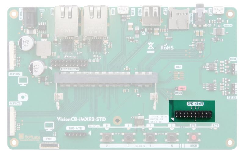
| Pin | Signal | MPU pin name | Description |
|---|---|---|---|
| 1 | GND | - | - |
| 2 | SPI5.SCK | GPIO2_IO21 | Line with optional GPIO functions |
| 3 | SPI7.SCK | GPIO2_IO07 | Line with optional GPIO functions |
| 4 | SPI5.MOSI | GPIO2_IO20 | Line with optional GPIO functions |
| 5 | SPI7.MOSI | GPIO2_IO06 | Line with optional GPIO functions |
| 6 | SPI5.MISO | GPIO2_IO19 | Line with optional GPIO functions |
| 7 | SPI7.MISO | PIO2_IO05 | Line with optional GPIO functions |
| 8 | SPI5.CS0 | GPIO2_IO18 | Line with optional GPIO functions |
| 9 | SPI7.CS0 | GPIO2_IO04 | Line with optional GPIO functions |
| 10 | I2C8.SDA | GPIO2_IO12 | 4.7 kOhm pull-up resistor connected to VDD-3V3 |
| 11 | I2C8.SCL | GPIO2_IO13 | 4.7 kOhm pull-up resistor connected to VDD-3V3 |
| 12 | I2C2.SDA | GPIO1_IO03 | 4.7 kOhm pull-up resistor connected to VDD-3V3 |
| 13 | UART7.TXD | GPIO2_IO08 | Line with optional GPIO functions |
| 14 | I2C2.SCL | GPIO1_IO02 | 4.7 kOhm pull-up resistor connected to VDD-3V3 |
| 15 | UART7.RTS | GPIO2_11 | Line with optional GPIO functions |
| 16 | I2C1.SDA | I2C1_SDA | Line pulled-up on the VisionSOM-iMX93 |
| 17 | UART7.CTS | GPIO2_10 | Line with optional GPIO functions |
| 18 | I2C1.SCL | I2C1_SCL | Line pulled-up on the VisionSOM-iMX93 |
| 19 | UART7.RXD | GPIO2_IO09 | Line with optional GPIO functions |
| 20 | VDD-3V3 | - | - |
Note:
1. The connector pins are numbered in the zig-zag style.
2. First connector pin is marked with an arrow.
1Gb Ethernet interfaces
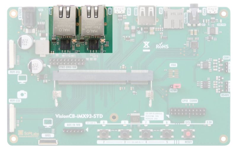
Ethernet channel 1
| Signal | MPU pin name | Description |
|---|---|---|
| ENET1.RXD3 | ENET1_RD3 | 1.8V Power Domain, alternative GPIO functions available |
| ENET1.RXD2 | ENET1_RD2 | 1.8V Power Domain, alternative GPIO functions available |
| ENET1.RXD1 | ENET1_RD1 | 1.8V Power Domain, alternative GPIO functions available |
| ENET1.RXD0 | ENET1_RD0 | 1.8V Power Domain, alternative GPIO functions available |
| ENET1.RXC | ENET1_RXC | 1.8V Power Domain, alternative GPIO functions available |
| ENET1.RX-CTL | ENET1_RXC_CTL | 1.8V Power Domain, alternative GPIO functions available |
| ENET1.TXD3 | ENET1_TD3 | 1.8V Power Domain, alternative GPIO functions available |
| ENET1.TXD2 | ENET1_TD2 | 1.8V Power Domain, alternative GPIO functions available |
| ENET1.TXD1 | ENET1_TD1 | 1.8V Power Domain, alternative GPIO functions available |
| ENET1.TXD0 | ENET1_TD0 | 1.8V Power Domain, alternative GPIO functions available |
| ENET1.TXC | ENET1_TXC | 1.8V Power Domain, alternative GPIO functions available |
| ENET1.TX-CTL | ENET1_TX_CTL | 1.8V Power Domain, alternative GPIO functions available |
| ENET1.MDC | ENET1_MDC | 1.8V Power Domain, alternative GPIO functions available |
| ENET1.MDIO | ENET1_MDIO | 1.8V Power Domain, alternative GPIO functions available |
| ENET1.INT | CCM_CLKO4 | 1.8V Power Domain, alternative GPIO functions available |
| ENET1.RESET | CCM_CLKO3 | 1.8V Power Domain, alternative GPIO functions available |
Ethernet channel 2
| Signal | MPU pin name | Description |
|---|---|---|
| ENET2.RXD3 | ENET2_RD3 | 1.8V Power Domain, alternative GPIO functions available |
| ENET2.RXD2 | ENET2_RD2 | 1.8V Power Domain, alternative GPIO functions available |
| ENET2.RXD1 | ENET2_RD1 | 1.8V Power Domain, alternative GPIO functions available |
| ENET2.RXD0 | ENET2_RD0 | 1.8V Power Domain, alternative GPIO functions available |
| ENET2.RXC | ENET2_RXC | 1.8V Power Domain, alternative GPIO functions available |
| ENET2.RX-CTL | ENET2_RXC_CTL | 1.8V Power Domain, alternative GPIO functions available |
| ENET2.TXD3 | ENET2_TD3 | 1.8V Power Domain, alternative GPIO functions available |
| ENET2.TXD2 | ENET2_TD2 | 1.8V Power Domain, alternative GPIO functions available |
| ENET2.TXD1 | ENET2_TD1 | 1.8V Power Domain, alternative GPIO functions available |
| ENET2.TXD0 | ENET2_TD0 | 1.8V Power Domain, alternative GPIO functions available |
| ENET2.TXC | ENET2_TXC | 1.8V Power Domain, alternative GPIO functions available |
| ENET2.TX-CTL | ENET2_TX_CTL | 1.8V Power Domain, alternative GPIO functions available |
| ENET2.MDC | ENET2_MDC | 1.8V Power Domain, alternative GPIO functions available |
| ENET2.MDIO | ENET2_MDIO | 1.8V Power Domain, alternative GPIO functions available |
| ENET1.INT | CCM_CLKO2 | 1.8V Power Domain, alternative GPIO functions available |
| ENET2.RESET | CCM_CLKO1 | 1.8V Power Domain, alternative GPIO functions available |
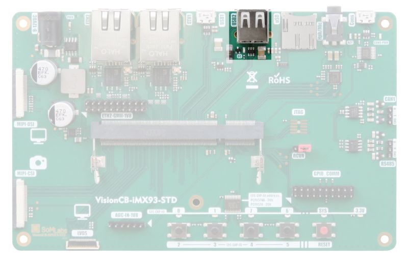
USB 2.0 (host)
| Signal | MPU pin name | Description |
|---|---|---|
| USB2.VBUS | USB2_VBUS | 5V compatible |
| USB2.VBUS-EN | GPIO2_IO23 | USB power switch enable line |
| USB2.VBUS-OC | SD2_RESET_B | Overcurrent signalling input with internal pull-up |
| USB2.D_N | USB2_D_N | Analog USB transceiver line |
| USB2.D_P | USB2_D_P | Analog USB transceiver line |
Note:
1. USB2 is configured as the host interface on VisionCB-iMX93-STD board.
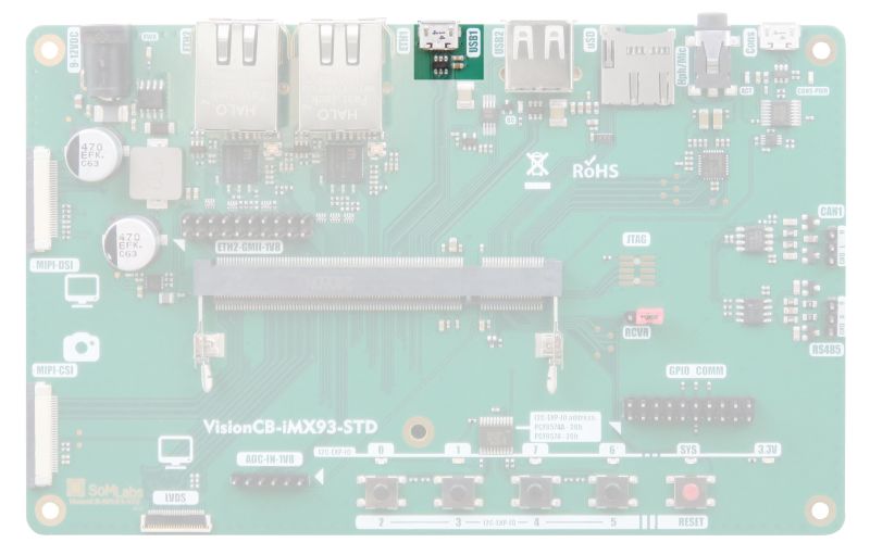
USB-OTG
| Signal | MPU pin name | Description |
|---|---|---|
| USB1.VBUS | USB1_VBUS | 5V compatible |
| USB1.VBUS-EN | GPIO2_IO22 | USB power switch enable line |
| USB1.VBUS-OC | SD_CD_B | Overcurrent signalling input with internal pull-up |
| USB1.ID | USB1_ID | OTG ID input with internal pull-up |
| USB1.D_N | USB1_D_N | Analog USB transceiver line |
| USB1.D_P | USB1_D_P | Analog USB transceiver line |
Note:
1. USB1 is configured as the OTG interface on VisionCB-iMX93-STD board.
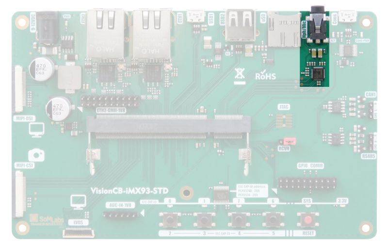
Audio codec
| Signal | MPU pin name | Description |
|---|---|---|
| SAI1.MCLK | UART2_RXD | Master clock for audio codec |
| SAI1.BCLK | SAI1_TXC | Bit clock for audio codec |
| SAI1.SYNC | SAI1_TXFS | L and R bit frames selector |
| SAI1.TXD | SAI1_TXD0 | Tx data line |
| SAI1.RXD | SAI1_RXD0 | Rx data line |
| I2C8.SCL | GPIO2_IO13 | Audio codec configuration I2C interface Pulled-up with 4.7 kOhm |
| I2C8.SDA | GPIO2_IO12 | Audio codec configuration I2C interface Pulled-up with 4.7 kOhm |
Note:
1. Audio codec is configured via I2C8 MPU interface.
2. Interface I2C8 is also used for on-board GPIO expander (PCF8574 or PCF8574A).
CAN interface
| Signal | MPU pin name | Description |
|---|---|---|
| CAN1.TX | PDM_CLK | Tx line |
| CAN1.RX | PDM_BIT_STREAM0 | Rx line |
| UART5.CTS | GPIO2_IO02 | Optional STB line of MCP2542FD1 |
Note:
1. STB line of MCP2542FD is pulled-down with 10kOhm resistor by default.
2. The PHY of CAN interface is MCP2542FD by Microchip.
RS-485 interface
| Signal | MPU pin name | Description |
|---|---|---|
| UART5.RXD | GPIO2_IO01 | Tx line |
| UART5.TXD | GPIO2_IO00 | Rx line |
| UART5.RTS | GPIO2_IO03 | Data Enable line, connected to DE of MAX3485CSA |
Note:
1. The PHY of RS-485 is MAX3485CSA or similar.
MicroSD socket
| Signal | MPU pin name | Description |
|---|---|---|
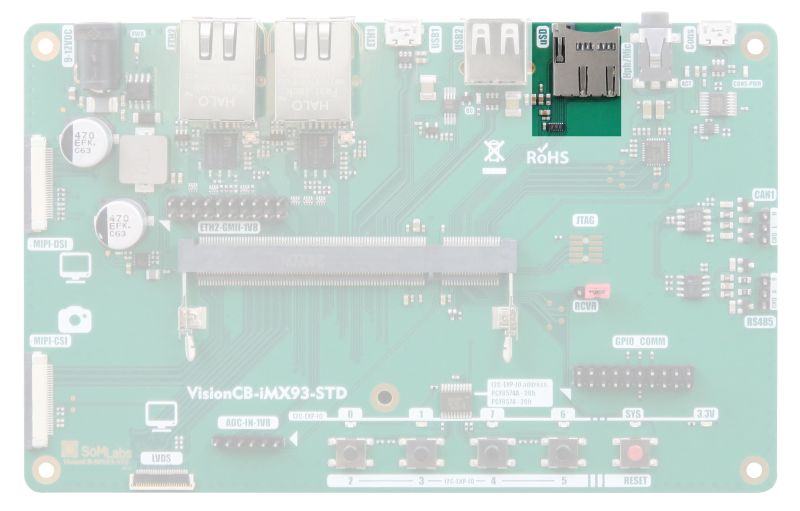
| SD2.NVCC | GPIO2_IO01 | 1.8V/3.3V power supply for SD card |
| SD2.DATA3 | SD2_DATA3 | SD bi-dir data line |
| SD2.DATA2 | SD2_DATA2 | SD bi-dir data line |
| SD2.DATA1 | SD2_DATA1 | SD bi-dir data line |
| SD2.DATA0 | SD2_DATA0 | SD bi-dir data line |
| SD2.CLK | SD2_CLK | SD interface clock line |
| SD2.CMD | SD2_CMD | SD interface command line |
User Interface (switches)
| Switch/Function | GPIO expander pin name | Description |
|---|---|---|
| 2/- | GPIO2 | Pulled-up with 47kOhm |
| 3/- | GPIO3 | Pulled-up with 47kOhm |
| 4/- | GPIO4 | Pulled-up with 47kOhm |
| 5/- | GPIO5 | Pulled-up with 47kOhm |
| -/GPIO2-IO27 | nINT | GPIO expander interrupt line |
Note:
1. Switches are connected to MPU via PCF8574A GPIO expander.
2. The base I2C address of PCF8574A GPIO expander is 38h.
3. Optionally as GPIO expander can be used PCF8574 with base I2C address 20h.
4. GPIO expander is connected to MPU via I2C8 interface (the same like in audio codec, interface lines are pulled-up with 4.7 kOhm).
5. The GPIO expander interrupt output is connected to GPIO2_IO27 GPIO of MPU.
User Interface (LEDs)
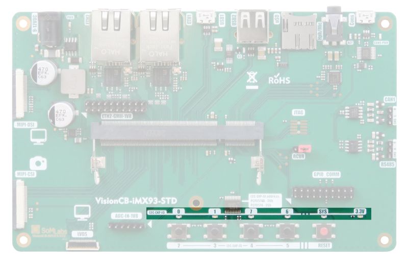
| Switch/Function | GPIO expander pin name | Description |
|---|---|---|
| 7/- | GPIO7 | - |
| 6/- | GPIO6 | - |
| 1/- | GPIO1 | - |
| 0/- | GPIO0 | - |
| -/GPIO2_IO27 | nINT | GPIO expander interrupt line |
Note:
1. LEDs are connected to MPU via PCF8574A GPIO expander.
2. The base I2C address of PCF8574A GPIO expander is 38h.
3. Optionally as GPIO expander can be used PCF8574 with base I2C address 20h.
4. GPIO expander is connected to MPU via I2C8 interface (the same like in audio codec, interface lines are pulled-up with 4.7 kOhm).
5. The GPIO expander interrupt output is connected to GPIO2_IO27 GPIO of MPU.
| Function | MPU pin name | Description |
|---|---|---|
| SYS-LED | PDM_BIT_STREAM1 | System heart-beat Logic levels from MPU are inverted by LED driver |
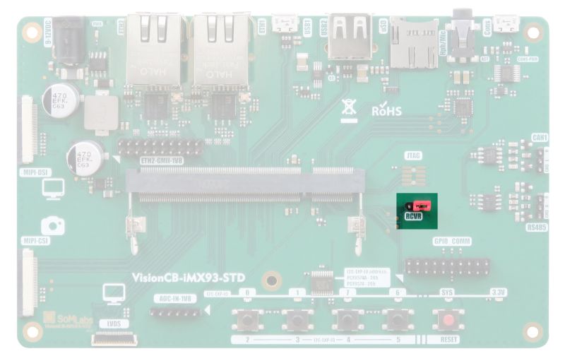
RECOVERY jumper
Dimensions
