VisionSOM-iMX93 Datasheet and Pinout
From SomLabs Wiki

VisionSOM-iMX93 Datasheet and Pinout
General description
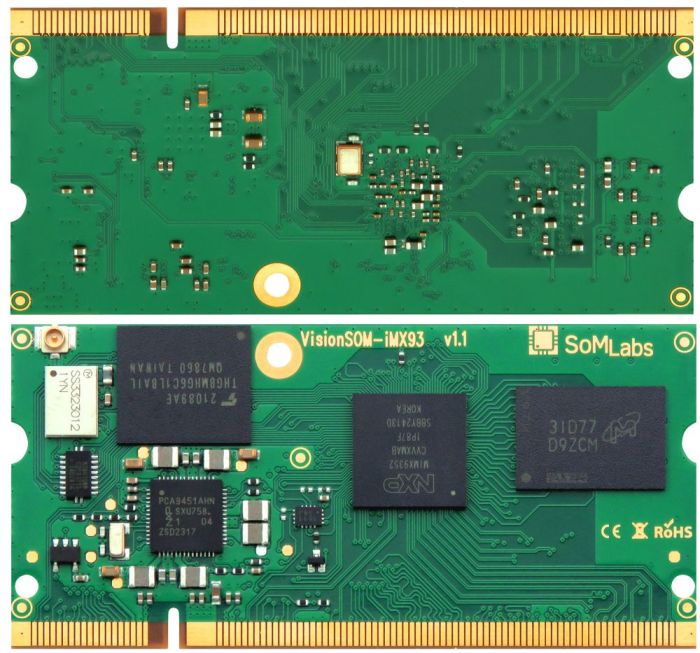
The VisionSOM-iMX93 (SLS26) family is a SODIMM-sized SoM based on the NXP iMX93 application processor which features a heterogeneous dual cores ARM Cortex-A55 (up to 1.7GHz) together with an ARM Cortex-M33 MCU core (up to 250 MHz) as well as an advanced 2D graphics processing unit (PXP) and neural network/machine learning coprocessor (NPU).
The dual Cortex-A55 and single Cortex-M33 based VisionSOM provides full flexibility to support real time application while supporting Linux, advanced HMI and AI/ML.
The VisionSOM-iMX93 (SLS26) is a general-purpose highly integrated SoM (System on Module). The module is featuring high computation power inculding AI and ML coprocessor. The option is fully certified Wi-Fi (802.11b/g/n) and Bluetooth (BLE 5.1) module. This module simplifies the carrier board design and is ideally suited for wireless application. The VisionSOM-iMX93 provides a variety memory configuration, including flexible range of LPDDR4 and eMMC Flash.
The VisionSOM-iMX93 supports connections to a variety of interfaces:
- two high-speed USB on-the-go with PHY,
- 2 x 1Gbit/s Ethernet,
- modern I3C and all classic serial interfaces,
- advanced Full HD display MIPI-DSI and HD LVDS interfaces,
- automotive CAN-FD interfaces.
In addition, the system supports industrial grade embedded applications.
SoMLabs also provides a complete hardware and software development board for the SoM in the form of a carrier board and optional TFT display and touch panel.
Applications
- Low-cost Gateway
- Domain Controller Compute Off-load Engine
- Human-machine Interfaces (HMI)
- Public Address Systems
- Home Appliances
- Home Automation – Smart Home
- IoT gateways
- Wireless or Networked Speakers
- Residential gateways
- Industrial embedded Linux computer
- Fitness/outdoor equipment
Features
- Powered by NXP i.MX9352 application processor
- Dual core ARM Cortex-A55 (at speed up to 1.7GHz)
- ARM Cortex-M33 core (at speed up to 250MHz)
- Built-in energy efficient NPU AI/ML coprocessor (Ethos U-65 microNPU)
- Up to 4GB LPDDR4
- Up to 32GB eMMC memory card
- MIPI-DSI interface (FullHD, 4 lane)
- LVDS display interface (HD, 4 lane)
- Parallel 24-bit RGB display interface
- MIPI-CSI interface (2 lane)
- 2 x 1Gbit Ethernet
- up to 2 x CAN-FD
- up to 2 x I3C serial interfaces
- up to 8 x UARTs
- up to 8 x low power SPI
- up to 8 x I2C
- Optional Murata 802.11b/g/n Wi-Fi and Bluetooth v5.1 module
- Power-efficient and cost-optimized solution
- Ideal for industrial IoT and embedded applications
- Integrated security features
- Yocto/Debian support
Pictures of SOM versions
| Version | Photo |
|---|---|
| eMMC |
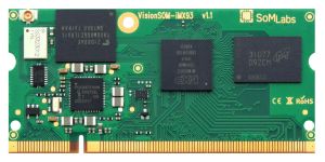 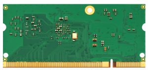 |
| WiFi/BT module is available for all memory configurations. |
Ordering info
| SLS | Product type SLS - System on Module |
| N | SOM Name 2 - High Performance VisionSOM SODIMM200 module |
| N | CPU Family 6 - i.MX 93 |
| CpuType | CPU Type X93DCN - i.MX 93 Dual Core with NPU |
| Clock | CPU Clock Speed 1700C - 1.7GHz (Industrial temperature range) |
| RamSize | LPDDR4 RAM Size 01GR - 1GB (1024MB) 02GR - 2GB (2048MB) 04GR - 4GB (4096MB) |
| FlashSize | eMMC Memory Size 04GE - 4GB eMMC 08GE - 8GB eMMC 16GE - 16GB eMMC 32GE - 32GB eMMC |
| SF | Special Features 0SF - No Special Features 1WB - Built-in dual-band Wi-Fi and Bluetooth v5.1 |
| TEMP | Operating Temperature E - Extended: -30 to +85 C I - Industrial: -40 to +85 C |
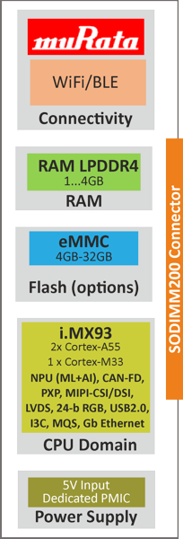
Block Diagram
Operating ranges
| Parameter | Value | Unit | Comment |
|---|---|---|---|
| Power Supply | Connected to VDD 5V SODIM200 pins | ||
| Max. input GPIO voltage | - | ||
| Environment temperature1 | oC | Industrial range w/o WiFi module | |
| Industrial range with WiFi module |
Note:
1. Maximum MPU junction temperature is +105oC.
2. Junction temperature determines MPU lifetime. Details: NXP AN13214 Application Note.
Electrical parameters
| SOM signal name |
Parameter | Value | Unit | ||
|---|---|---|---|---|---|
| Min. | Typ. | Max. | |||
| VDD-5V | Supply Voltage (Input) | 4.0 | 5.0 | 5.25 | V |
| SD1-NVCC | Output power supply for external 1.8/3.3V accesories | - | - | 0.08 | A |
| VDD-1V8 | Output power supply for external 1.8V accesories | - | - | 0.4 | A |
| VDD-3V3 | Output power supply for external 3.3V accesories | - | - | 0.31 | A |
| VGPIO @1V8 | GPIO Input Voltage | 0 | - | 2.05 | V |
| VGPIO @3V3 | GPIO Input Voltage | 0 | - | 3.62 | V |
| VUSB_VBUS | USB VBUS Input Voltage | 0 | - | 5.03 | V |
Notes:
1. Total current on both VDD-3V3 outputs.
2. Applying the maximum voltage 3.6V results in shorten lifetime. Recommended value is smaller than 3.45V.
3. Allowed maximum voltage range of USBx_VBUS input is 0...+3.95V but input current is limited by 30k resistor connected in series.
SoM pinout
Important notes:
1. Detail pin configurations description you can find, edit and arrange in dedicated MEX file (with free "iMX PinTool" configurational tool).
2. Following MPU lines are dual use:
* UART1_TXD (ball E21) - BOOT3 during MPU reset/after reset: UART1_TXD
* UART2_TXD (ball F21) - BOOT2 during MPU reset/after reset: GPIO1_IO07
* SAI1_TXD0 (ball H21) - BOOT1 during MPU reset/after reset: SAI1.TXD
* SAI1_TXFS (ball G21) - BOOT0 during MPU reset/after reset: SAI1.SYNC
3. RECOVERY line -> BOOT3
4. BOOT2...BOOT0 are premanently connected to GND
5. SDIO3 interface is used to communication with Murata 1DX radio module
6. eMMC memory is connected to SDIO1 interface
| SOM pin number | MPU pin name | SOM pin name | GPIO | FCBGA306 ball number | Notes |
|---|---|---|---|---|---|
| 1 | - | GND | - | - | - |
| 2 | - | GND | - | - | - |
| 3 | GPIO2_IO12 | I2C8.SDA | GPIO2_IO12 | N20 | 3.3V power domain |
| 4 | - | - | - | - | - |
| 5 | GPIO2_IO13 | I2C8.SCL | GPIO2_IO13 | N21 | 3.3V power domain |
| 6 | - | RECOVERY | - | BOOT MODE selection, if: RECOVERY = "0" then BOOT0 = "1", as a result serial loader starts RECOVERY = "1" or open then BOOT0 = "0", as a result MCU boots from fuses. | |
| 7 | - | GND | - | - | - |
| 8 | ONOFF | PWR-ON | - | A19 | 1.8V power domain A brief connection the PWR-ON to GND in the OFF mode causes the internal power management state machine to change the state to ON. In the ON mode, a brief connection the PWR-ON to GND generates an interrupt (intended to be a software-controllable power-down). Approximately five seconds (or more) to GND causes a forced OFF. |
| 9 | UART2_RXD | SAI1.MCLK | GPIO1_IO06 | F20 | 3.3V power domain |
| 10 | - | RESET-OUT | - | - | 3.3V power domain Open-drain system reset output |
| 11 | SAI1_TXD0 | SAI1.TXD | GPIO1_IO13 | H21 | 3.3V power domain If POR-B="0" then this pin acts as BOOT1 input (by default ="0") |
| 12 | - | RESET-IN | - | - | 3.3V power domain PMIC_RST_B input of PCA9451AHN on-board PMIC Active low global reset line (hard reset by turning off the power) |
| 13 | SAI1_RXD0 | SAI1.RXD | GPIO1_IO14 | H20 | 3.3V power domain |
| 14 | - | GND | - | - | - |
| 15 | SAI1_TXC | SAI1.BCLK | GPIO1_IO12 | G20 | 3.3V power domain |
| 16 | DAP_TMS_SWDIO | JTAG.TMS | GPIO3_IO29 | W2 | 1.8V power domain |
| 17 | SAI1_TXFS | SAI1.SYNC | GPIO1_IO11 | G21 | 3.3V power domain If POR-B="0" then this pin acts as BOOT0 input (by default ="0") |
| 18 | DAP_TCLK_SWCLK | JTAG.TCK | GPIO3_IO30 | Y1 | 1.8V power domain |
| 19 | - | GND | - | - | - |
| 20 | DAP_TDO_TRACESWO | JTAG.TDO | GPIO3_IO31 | Y2 | 1.8V power domain |
| 21 | SD2_DATA1 | SD2.DATA1 | GPIO3_IO04 | AA18 | 1.8V or 3.3V power domain for SDIO2 interface, selected by software with SDIO-VSELECT pin. Output is 3.3 V when SDIO-VSELECT is driven LOW and 1.8 V when driven HIGH. |
| 22 | DAP_TDI | JTAG.TDI | GPIO4_IO05 | W11 | 1.8V power domain |
| 23 | SD2_DATA0 | SD2.DATA0 | GPIO3_IO03 | Y18 | 1.8V or 3.3V power domain for SDIO2 interface, selected by software with SDIO-VSELECT pin. Output is 3.3 V when SDIO-VSELECT is driven LOW and 1.8 V when driven HIGH. |
| 24 | TAMPER0 | TAMPER0 | - | F14 | 1.8V power domain |
| 25 | - | GND | - | - | - |
| 26 | TAMPER1 | TAMPER1 | - | B16 | 1.8V power domain |
| 27 | SD2_CLK | SD2.CLK | GPIO3_IO01 | AA19 | 1.8V or 3.3V power domain for SDIO2 interface, selected by software with SDIO-VSELECT pin. Output is 3.3 V when SDIO-VSELECT is driven LOW and 1.8 V when driven HIGH. |
| 28 | UART1_RXD | UART1.RXD | GPIO1_IO04 | E20 | 3.3V power domain |
| 29 | SD2_CMD | SD2.CMD | GPIO3_IO02 | Y19 | 1.8V or 3.3V power domain for SDIO2 interface, selected by software with SDIO-VSELECT pin. Output is 3.3 V when SDIO-VSELECT is driven LOW and 1.8 V when driven HIGH. |
| 30 | UART1_TXD | UART1.TXD | GPIO1_IO05 | E21 | 3.3V power domain If POR-B="0" then this pin acts as BOOT1 input (depends on RECOVERY line state) |
| 31 | SD2_DATA3 | SD2.DATA3 | GPIO3_IO06 | AA20 | 1.8V or 3.3V power domain for SDIO2 interface, selected by software with SDIO-VSELECT pin. Output is 3.3 V when SDIO-VSELECT is driven LOW and 1.8 V when driven HIGH. |
| 32 | PDM_BIT_STREAM1 | SYS-LED | GPIO1_IO10 | G18 | 3.3V power domain |
| 33 | SD2_DATA2 | SD2.DATA2 | GPIO3_IO05 | Y20 | 1.8V or 3.3V power domain for SDIO2 interface, selected by software with SDIO-VSELECT pin. Output is 3.3 V when SDIO-VSELECT is driven LOW and 1.8 V when driven HIGH. |
| 34 | - | - | - | - | - |
| 35 | - | SD2.NVCC | - | - | 1.8V or 3.3V power supply for SDIO2 interface, selected by software with SDIO-VSELECT pin. Output is 3.3 V when SDIO-VSELECT is driven LOW and 1.8 V when driven HIGH. |
| 36 | - | - | - | - | - |
| 37 | - | GND | - | - | - |
| 38 | - | GND | - | - | - |
| 39 | - | VDD-1V8 | - | - | Internally generated by PMIC 1.8V for internal peripherals by BUCK5 channel (maximum external load is limted, details in Electrical Characteristics section of "PCA9451 Product data sheet" by NXP) |
| 40 | - | VDD-1V8 | - | - | Internally generated by PMIC 1.8V for internal peripherals by BUCK5 channel (maximum external load is limted, details in Electrical Characteristics section of "PCA9451 Product data sheet" by NXP) |
| 41 | - | VDD-5V0 | - | - | Power supply input |
| 42 | - | VDD-5V0 | - | - | Power supply input |
| 43 | - | VDD-5V0 | - | - | Power supply input |
| 44 | - | VDD-5V0 | - | - | Power supply input |
| 45 | - | VDD-5V0 | - | - | Power supply input |
| 46 | - | VDD-5V0 | - | - | Power supply input |
| 47 | - | VDD-5V0 | - | - | Power supply input |
| 48 | - | VDD-5V0 | - | - | Power supply input |
| 49 | - | VDD-5V0 | - | - | Power supply input |
| 50 | - | VDD-5V0 | - | - | Power supply input |
| 51 | - | - | - | - | - |
| 52 | - | - | - | - | - |
| 53 | - | VDD-3V3 | - | - | Internally generated by PMIC 3.3V for internal peripherals by BUCK4 channel (maximum external load is limted, details in Electrical Characteristics section of "PCA9451 Product data sheet" by NXP) |
| 54 | - | VDD-3V3 | - | - | Internally generated by PMIC 3.3V for internal peripherals by BUCK4 channel (maximum external load is limted, details in Electrical Characteristics section of "PCA9451 Product data sheet" by NXP) |
| 55 | - | GND | - | - | - |
| 56 | - | - | - | - | - |
| 57 | USB2_ID | USB2.ID | - | E12 | 3.3V power domain |
| 58 | - | GND | - | - | - |
| 59 | USB2_D_N | USB2.D_N | - | A15 | USB2 interface analog I/O |
| 60 | - | - | - | - | - |
| 61 | USB2_D_P | USB2.D_P | - | B15 | USB2 interface analog I/O |
| 62 | - | - | - | - | - |
| 63 | USB2_VBUS | USB2.VBUS | - | E14 | USB2 interface analog input (5V compatible) |
| 64 | - | - | - | - | - |
| 65 | SD2_RESET_B | USB2.VBUS-OC | GPIO3_IO07 | AA17 | 3.3V power domain |
| 66 | - | - | - | - | - |
| 67 | GPIO2_IO23 | USB2.VBUS-EN | GPIO2_IO23 | U20 | 3.3V power domain |
| 68 | GPIO2_IO27 | GPIO2-IO27 | GPIO2_IO27 | W21 | 3.3V power domain |
| 69 | - | GND | - | - | - |
| 70 | - | GND | - | - | - |
| 71 | GPIO2_IO22 | USB1.VBUS-EN | GPIO2_IO22 | U18 | 3.3V power domain |
| 72 | GPIO1_IO02 | I2C2.SCL | GPIO1_IO02 | D20 | 3.3V power domain |
| 73 | SD_CD_B | USB1.VBUS-OC | GPIO3_IO00 | Y17 | 3.3V power domain |
| 74 | GPIO1_IO03 | I2C2.SDA | GPIO1_IO03 | D21 | 3.3V power domain |
| 75 | USB1_VBUS | USB1.VBUS | - | F12 | USB1 interface analog input (5V compatible) |
| 76 | - | GND | - | - | - |
| 77 | - | - | - | - | - |
| 78 | UART2_TXD | GPIO1-IO07 | GPIO1_IO07 | F21 | 3.3V power domain If POR-B="0" then this pin acts as BOOT2 input (by default ="0") |
| 79 | - | - | - | - | - |
| 80 | PDM_BIT_STREAM0 | CAN1.RX | GPIO1_IO09 | J17 | 3.3V power domain |
| 81 | - | GND | - | - | - |
| 82 | PDM_CLK | CAN1.TX | GPIO1_IO08 | G17 | 3.3V power domain |
| 83 | - | - | - | - | - |
| 84 | - | GND | - | - | - |
| 85 | - | - | - | - | - |
| 86 | GPIO2_IO18 | SPI5.CS0 | GPIO2_IO18 | R18 | 3.3V power domain |
| 87 | USB1_ID | USB1.ID | - | C11 | 3.3V power domain |
| 88 | GPIO2_IO21 | SPI5.SCK | GPIO2_IO21 | T21 | 3.3V power domain |
| 89 | USB1_D_N | USB1.D_N | - | A14 | USB1 interface analog I/O |
| 90 | GPIO2_IO20 | SPI5.MOSI | GPIO2_IO20 | T20 | 3.3V power domain |
| 91 | USB1_D_P | USB1.D_P | - | B14 | USB1 interface analog I/O |
| 92 | GPIO2_IO19 | SPI5.MISO | GPIO2_IO19 | R17 | 3.3V power domain |
| 93 | - | GND | - | - | - |
| 94 | - | GND | - | - | - |
| 95 | CCM_CLKO3 | ENET1.RESET | GPIO4_IO28 | U4 | 1.8V power domain |
| 96 | GPIO2_10 | UART7.CTS | GPIO2_IO10 | N17 | 3.3V power domain |
| 97 | CCM_CLKO4 | ENET1.INT | GPIO4_IO29 | V4 | 1.8V power domain |
| 98 | GPIO2_11 | UART7.RTS | GPIO2_IO11 | N18 | 3.3V power domain |
| 99 | ENET1_MDIO | ENET1.MDIO | GPIO4_IO01 | AA10 | 1.8V power domain |
| 100 | GPIO2_IO08 | UART7.TXD | GPIO2_IO08 | M20 | 3.3V power domain |
| 101 | ENET1_MDC | ENET1.MDC | GPIO4_IO00 | AA11 | 1.8V power domain |
| 102 | GPIO2_IO09 | UART7.RXD | GPIO2_IO09 | M21 | 3.3V power domain |
| 103 | - | GND | - | - | - |
| 104 | - | GND | - | - | - |
| 105 | ENET1_RXC | ENET1.RXC | GPIO4_IO09 | AA7 | 1.8V power domain |
| 106 | GPIO2_IO02 | UART5.CTS | GPIO2_IO02 | K20 | 3.3V power domain |
| 107 | ENET1_RX_CTL | ENET1.RX-CTL | GPIO4_IO08 | Y8 | 1.8V power domain |
| 108 | GPIO2_IO03 | UART5.RTS | GPIO2_IO03 | K21 | 3.3V power domain |
| 109 | ENET1_RD0 | ENET1.RXD0 | GPIO4_IO10 | AA8 | 1.8V power domain |
| 110 | GPIO2_IO00 | UART5.TXD | GPIO2_IO00 | J21 | 3.3V power domain |
| 111 | ENET1_RD1 | ENET1.RXD1 | GPIO4_IO11 | Y9 | 1.8V power domain |
| 112 | GPIO2_IO01 | UART5.RXD | GPIO2_IO01 | J20 | 3.3V power domain |
| 113 | ENET1_RD2 | ENET1.RXD2 | GPIO4_IO12 | AA9 | 1.8V power domain |
| 114 | - | GND | - | - | - |
| 115 | ENET1_RD3 | ENET1.RXD3 | GPIO4_IO13 | Y10 | 1.8V power domain |
| 116 | ADC_IN3 | ADC.IN3 | - | B21 | 12-b ADC input Input voltage range 0…1.8V |
| 117 | - | GND | - | - | - |
| 118 | ADC_IN2 | ADC.IN2 | - | B20 | 12-b ADC input Input voltage range 0…1.8V |
| 119 | ENET1_TX_CTL | ENET1.TX-CTL | GPIO4_IO06 | V10 | 1.8V power domain |
| 120 | ADC_IN1 | ADC.IN1 | - | A20 | 12-b ADC input Input voltage range 0…1.8V |
| 121 | ENET1_TXC | ENET1.TXC | GPIO4_IO07 | U10 | 1.8V power domain |
| 122 | ADC_IN0 | ADC.IN0 | - | B19 | 12-b ADC input Input voltage range 0…1.8V |
| 123 | ENET1_TD3 | ENET1.TXD3 | GPIO4_IO02 | V12 | 1.8V power domain |
| 124 | - | GND | - | - | - |
| 125 | ENET1_TD2 | ENET1.TXD2 | GPIO4_IO03 | U12 | 1.8V power domain |
| 126 | GPIO2_IO04 | SPI7.CS0 | GPIO2_IO04 | L17 | 3.3V power domain |
| 127 | ENET1_TD1 | ENET1.TXD1 | GPIO4_IO02 | T12 | 1.8V power domain |
| 128 | GPIO2_IO07 | SPI7.SCK | GPIO2_IO07 | L21 | 3.3V power domain |
| 129 | ENET1_TD0 | ENET1.TXD0 | GPIO4_IO05 | W11 | 1.8V power domain |
| 130 | GPIO2_IO06 | SPI7.MOSI | GPIO2_IO06 | L20 | 3.3V power domain |
| 131 | - | GND | - | - | - |
| 132 | GPIO2_IO05 | SPI7.MISO | GPIO2_IO05 | L18 | 3.3V power domain |
| 133 | CCM_CLKO1 | ENET2.RESET | GPIO3_IO26 | AA2 | 1.8V power domain |
| 134 | - | GND | - | - | - |
| 135 | CCM_CLKO2 | ENET2.INT | GPIO3_IO27 | Y3 | 1.8V power domain |
| 136 | I2C1_SDA | I2C1.SDA | GPIO1_IO01 | C21 | 3.3V power domain Internally used for PCA9451AHN PMIC The line is pulled to 3.3V with 4.7kOhm resistors |
| 137 | ENET2_MDIO | ENET2.MDIO | GPIO4_IO15 | AA6 | 1.8V power domain |
| 138 | I2C1_SCL | I2C1.SCL | GPIO1_IO00 | C20 | 3.3V power domain Internally used for PCA9451AHN PMIC The line is pulled to 3.3V with 4.7kOhm resistors |
| 139 | ENET2_MDC | ENET2.MDC | GPIO4_IO14 | Y7 | 1.8V power domain |
| 140 | - | GND | - | - | - |
| 141 | - | GND | - | - | - |
| 142 | LVDS_DATA3_P | LVDS.DATA3_P | - | A3 | LVDS video output channel analog line |
| 143 | ENET2_RXC | ENET2.RXC | GPIO4_IO23 | AA3 | 1.8V power domain |
| 144 | LVDS_DATA3_N | LVDS.DATA3_N | - | B3 | LVDS video output channel analog line |
| 145 | ENET2_RX_CTL | ENET2.RX-CTL | GPIO4_IO22 | Y4 | 1.8V power domain |
| 146 | - | GND | - | - | - |
| 147 | ENET2_RD0 | ENET2.RXD0 | GPIO4_IO24 | AA4 | 1.8V power domain |
| 148 | LVDS_CLK_P | LVDS.CLK_P | - | B3 | LVDS video output channel analog line |
| 149 | ENET2_RD1 | ENET2.RXD1 | GPIO4_IO25 | Y5 | 1.8V power domain |
| 150 | LVDS_CLK_N | LVDS.CLK_N | - | A3 | LVDS video output channel analog line |
| 151 | ENET2_RD2 | ENET2.RXD2 | GPIO4_IO26 | AA5 | 1.8V power domain |
| 152 | - | GND | - | - | - |
| 153 | ENET2_RD3 | ENET2.RXD3 | GPIO4_IO27 | Y6 | 1.8V power domain |
| 154 | LVDS_DATA2_P | LVDS.DATA2_P | - | B1 | LVDS video output channel analog line |
| 155 | - | GND | - | - | - |
| 156 | LVDS_DATA2_N | LVDS.DATA2_N | - | C1 | LVDS video output channel analog line |
| 157 | ENET2_TX_CTL | ENET2.TX-CTL | GPIO4_IO20 | V6 | 1.8V power domain |
| 158 | - | GND | - | - | - |
| 159 | ENET2_TXC | ENET2.TXC | GPIO4_IO21 | U6 | 1.8V power domain |
| 160 | LVDS_DATA1_P | LVDS.DATA1_P | - | B4 | LVDS video output channel analog line |
| 161 | ENET2_TD3 | ENET2.TXD3 | GPIO4_IO16 | T10 | 1.8V power domain |
| 162 | LVDS_DATA1_N | LVDS.DATA1_N | - | A4 | LVDS video output channel analog line |
| 163 | ENET2_TD2 | ENET2.TXD2 | GPIO4_IO17 | V8 | 1.8V power domain |
| 164 | - | GND | - | - | - |
| 165 | ENET2_TD1 | ENET2.TXD1 | GPIO4_IO18 | U8 | 1.8V power domain |
| 166 | LVDS_DATA0_P | LVDS.DATA0_P | - | B5 | LVDS video output channel analog line |
| 167 | ENET2_TD0 | ENET2.TXD0 | GPIO4_IO19 | T8 | 1.8V power domain |
| 168 | LVDS_DATA0_N | LVDS.DATA0_N | - | A5 | LVDS video output channel analog line |
| 169 | - | GND | - | - | - |
| 170 | - | GND | - | - | - |
| 171 | DSI_DATA3_P | DSI.DATA3_P | - | B9 | DSI video output channel analog line |
| 172 | - | - | - | - | - |
| 173 | DSI_DATA3_N | DSI.DATA3_N | - | A9 | DSI video output channel analog line |
| 174 | - | - | - | - | - |
| 175 | - | GND | - | - | - |
| 176 | - | GND | - | - | - |
| 177 | DSI_DATA2_P | DSI.DATA2_P | - | B8 | DSI video output channel analog line |
| 178 | - | - | - | - | - |
| 179 | DSI_DATA2_N | DSI.DATA2_N | - | A8 | DSI video output channel analog line |
| 180 | - | - | - | - | - |
| 181 | - | GND | - | - | - |
| 182 | - | GND | - | - | - |
| 183 | DSI_CLK_P | DSI.CLK_P | - | E6 | DSI video output channel analog line |
| 184 | CSI_DATA1_N | CSI.DATA1_N | - | A10 | CSI video input channel analog line |
| 185 | DSI_CLK_N | DSI.CLK_N | - | D6 | DSI video output channel analog line |
| 186 | CSI_DATA1_P | CSI.DATA1_P | - | B10 | CSI video input channel analog line |
| 187 | - | GND | - | - | - |
| 188 | - | GND | - | - | - |
| 189 | DSI_DATA1_P | DSI.DATA1_P | - | B7 | DSI video output channel analog line |
| 190 | CSI_DATA0_N | CSI.DATA0_N | - | A11 | CSI video input channel analog line |
| 191 | DSI_DATA1_N | DSI.DATA1_N | - | A7 | DSI video output channel analog line |
| 192 | CSI_DATA0_P | CSI.DATA0_P | - | B11 | CSI video input channel analog line |
| 193 | - | GND | - | - | - |
| 194 | - | GND | - | - | - |
| 195 | DSI_DATA0_P | DSI.DATA0_P | - | B6 | DSI video output channel analog line |
| 196 | CSI_CLK_N | CSI.CLK_N | - | D10 | CSI video input channel analog line |
| 197 | DSI_DATA0_N | DSI.DATA0_N | - | A6 | DSI video output channel analog line |
| 198 | CSI_CLK_P | CSI.CLK_P | - | E10 | CSI video input channel analog line |
| 199 | - | GND | - | - | - |
| 200 | - | GND | - | - | - |
| GPIO2_IO14 | UART3.TXD | GPIO2_IO14 | P20 | BT communication interface (connected to BT_UART_RXD line of 1DX radio module) | |
| GPIO2_IO15 | UART3.RXD | GPIO2_IO15 | P21 | BT communication interface (connected to BT_UART_TXD line of 1DX radio module) | |
| GPIO2_IO16 | UART3.CTS | GPIO2_IO16 | R21 | BT communication interface (connected to BT_UART_CTS line of 1DX radio module) | |
| GPIO2_IO17 | UART3.RTS | GPIO2_IO17 | R20 | BT communication interface (connected to BT_UART_RTS line of 1DX radio module) | |
| GPIO2_IO24 | PMIC-INT | GPIO2_IO24 | U21 | PMIC interrupt line | |
| GPIO2_IO25 | BT-DEV-WAKE | GPIO2_IO25 | V21 | BT communication interface (connected to BT_DEV_WAKE line of 1DX radio module) | |
| GPIO2_IO26 | BT-H-WAKE | GPIO2_IO26 | V20 | BT communication interface (connected to BT_HOST_WAKE line of 1DX radio module) | |
| GPIO2_IO28 | BT-ENABLE | GPIO2_IO28 | W20 | BT communication interface (connected to BT_REG_ON line of 1DX radio module) | |
| GPIO2_IO29 | WLAN-ENABLE | GPIO2_IO29 | Y21 | Connected with WLAN-EN (WL_REG_ON) line of 1DX radio module | |
| SD2_VSELECT | SDIO-VSELECT | GPIO3_IO19 | V18 | 1.8V or 3.3V power domain for SDIO2 interface, selected by software with SDIO-VSELECT pin. Output is 3.3 V when SDIO-VSELECT is driven LOW and 1.8 V when driven HIGH. | |
| WDOG-ANY | WDOG-B | - | J18 | Internal hardware watchdog line (not available to the user) | |
| SD3_CLK | SD3-CLK | GPIO3_IO20 | V16 | SDIO3 interface line, connected with 1DX radio module (not available to the user) | |
| SD3_CMD | SD3-CMD | GPIO3_IO21 | U16 | SDIO3 interface line, connected with 1DX radio module (not available to the user) | |
| SD3_DATA0 | SD3-DATA0 | GPIO3_IO22 | T16 | SDIO3 interface line, connected with 1DX radio module (not available to the user) | |
| SD3_DATA1 | SD3-DATA1 | GPIO3_IO23 | V14 | SDIO3 interface line, connected with 1DX radio module (not available to the user) | |
| SD3_DATA2 | SD3-DATA2 | GPIO3_IO24 | U14 | SDIO3 interface line, connected with 1DX radio module (not available to the user) | |
| SD3_DATA3 | SD3-DATA3 | GPIO3_IO25 | T14 | SDIO3 interface line, connected with 1DX radio module (not available to the user) |
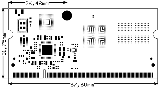
Dimensions
